Specific Process Knowledge/Etch/III-V ICP/InP-InGaAsP-InGaAs: Difference between revisions
No edit summary |
|||
| Line 61: | Line 61: | ||
===With InP piece on Si carrier=== | ===With InP piece on Si carrier=== | ||
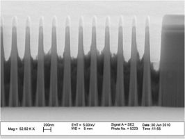
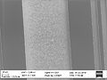
InP piece patterned with SiO2. The pice was etched on topof a Siwafer with out bonding. The InP etch was used. | InP piece patterned with SiO2. The pice was etched on topof a Siwafer with out bonding. The InP etch was used. | ||
<gallery | <gallery caption="Result of InP etching." width="5000px" height="4000px" perrow="3"> | ||
caption="Result of InP etching." | |||
Image:S1_00.jpg | Image:S1_00.jpg | ||
Image:S1_30dg_01.jpg | Image:S1_30dg_01.jpg | ||
Revision as of 13:14, 19 June 2018
Feedback to this page: click here
InP/InGaAsP/InGaAs etch
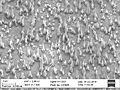
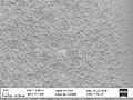
Unselective etch for large sized features and small aspect ratios by David Larsson, DTU Photonics, 2011
| Recipe | InP Etch 1/InP Precond 1 |
| Cl2 flow | 20 sccm |
| N2 flow | 40 sccm |
| Ar flow | 10 sccm |
| Platen power | 100 W |
| Coil power | 500 W |
| Pressure | 2 mTorr |
| Platen chiller temperature | 180 oC |
| Results (InP Etch 1) | |
| Etch rate | 500-600 nm/min |
| Sidewall angle | 86-87 o |
| Selectivity (InP:SiO2, InP:HSQ) | 50:1 |
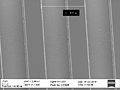
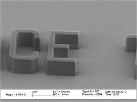
- Result of InP etching. David Larsson, DTU Photonics, 2011
-
-


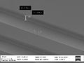
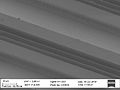
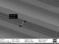
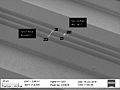
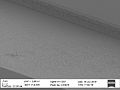
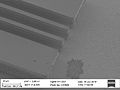
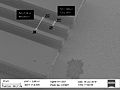
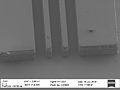
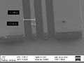
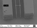
InP etching June 2018
With InP piece on Si carrier
InP piece patterned with SiO2. The pice was etched on topof a Siwafer with out bonding. The InP etch was used.
- Result of InP etching.
-
-
-
-
-
-
-
-
-
-
-
-
-
-
-