Specific Process Knowledge/Characterization/XPS: Difference between revisions
No edit summary |
|||
| Line 1: | Line 1: | ||
'''Feedback to this page''': '''[mailto:labadviser@danchip.dtu.dk?Subject=Feed%20back%20from%20page%20http://labadviser.danchip.dtu.dk/index.php?title=Specific_Process_Knowledge/Characterization/XPS click here]''' | '''Feedback to this page''': '''[mailto:labadviser@danchip.dtu.dk?Subject=Feed%20back%20from%20page%20http://labadviser.danchip.dtu.dk/index.php?title=Specific_Process_Knowledge/Characterization/XPS click here]''' | ||
<!--Checked for updates on 14/5-2018 - ok/jmli --> | |||
Revision as of 11:46, 14 May 2018
Feedback to this page: click here
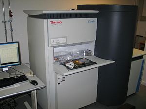
XPS-ThermoScientific

In the basement under the cleanroom an X-ray Photoelectron Spectroscopy (XPS) system is installed in room 904. It is a K-Alpha system by ThermoScientific that enables the users to perform elemental and chemical analysis of samples.
The user manual(s), user APV(s), technical information and contact information are be found in LabManager:
XPS-ThermoScientific in LabManager
Elemental analysis
The XPS instrument enables elemental analysis, chemical state analysis on the sample surface or deeper down by a depth profiling. A comparison about techniques and instruments used for elemental analysis at Danchip can be found on the page Element analysis.
More about the different possibilities of the XPS instrument is found here:
- XPS technique
- Elemental composition analysis
- Chemical state analysis
- Depth profiling
- Carbon contamination
Analyzing XPS spectra
The analysis of XPS spectra is an art in itself. Below is collection of examples (ehh..not yet but hopefully quite soon) in which the Avantage software package has been used to extract information from experiments.
Equipment performance of XPS-ThermoScientific
| Purpose | Chemical analysis |
|
|---|---|---|
| Performance | Spot size | Can be set between 30µm - 400µm |
| Probing depth | Depending on probed element. Max probe depth lies within 10-200 Å. | |
| Resolution | Dependent on probed elements. Concentrations down to about 0,5 atomic % can in some cases be detected. | |
| Charge compensation |
Flood gun can be used for charge compensation of non conductive samples | |
| Finding structures | Choose measuring spot from camera image (magnified) | |
| Depth profiling | Purpose | With ion beam etch the top layer of the material can be removed, to do a depth profiling |
| Ion beam size | About 3x1 mm | |
| Substrates | Substrate size |
Maximum 60x60 mm |
| Substrate thickness |
Maximum height about 20 mm |
