Specific Process Knowledge/Bonding/Wafer Bonder 02: Difference between revisions
Appearance
No edit summary |
|||
| Line 1: | Line 1: | ||
'''Feedback to this page''': '''[mailto:labadviser@danchip.dtu.dk?Subject=Feed%20back%20from%20page%20http://labadviser.danchip.dtu.dk/index.php/Specific_Process_Knowledge/Bonding/Wafer_Bonder_02 click here]''' | '''Feedback to this page''': '''[mailto:labadviser@danchip.dtu.dk?Subject=Feed%20back%20from%20page%20http://labadviser.danchip.dtu.dk/index.php/Specific_Process_Knowledge/Bonding/Wafer_Bonder_02 click here]''' | ||
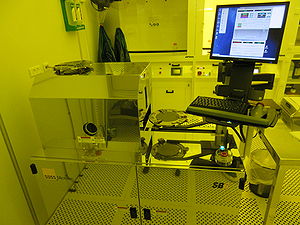
[[Image:wafer bonder2.jpg|300x300px|thumb|Wafer Bonder 02: Positioned in cleanroom E-4]] | |||
The Wafer bonder 02 is a system for bonding. 3 different types of [[Specific Process Knowledge/Bonding|bonding]] can be done: Anodic, Eutectic and Fusion. Furthermore it is possible to align the wafers one wishes to bond. It is also possible to process and align pieces. | The Wafer bonder 02 is a system for bonding. 3 different types of [[Specific Process Knowledge/Bonding|bonding]] can be done: Anodic, Eutectic and Fusion. Furthermore it is possible to align the wafers one wishes to bond. It is also possible to process and align pieces. | ||
| Line 9: | Line 9: | ||
<br clear="all" /> | <br clear="all" /> | ||
==Process information== | ==Process information== | ||
Revision as of 11:33, 19 May 2017
Feedback to this page: click here

The Wafer bonder 02 is a system for bonding. 3 different types of bonding can be done: Anodic, Eutectic and Fusion. Furthermore it is possible to align the wafers one wishes to bond. It is also possible to process and align pieces.
The user manual, quality control procedure and results, user APV(s), and contact information can be found in LabManager: Equipment info in LabManager
Process information
Types of Bonding
| Purpose | Bonding |
|
|---|---|---|
| Performance | Alignment accuracy |
|
| Process parameter range | Process Temperature |
|
| Process pressure |
| |
| Piston Force |
| |
| Substrates | Batch size |
|
| Substrate material allowed |
| |
| Material allowed on the substrate |
|
