LabAdviser/Technology Research/Fabrication of Hyperbolic Metamaterials using Atomic Layer Deposition/AZO gratings: Difference between revisions
| Line 4: | Line 4: | ||
The whole fabrication work took place in a class 100 cleanroom. First, standard double side polished Si (100) wafers were selected and RCA cleaned (optional). Conventional deep-UV lithography (DUV stepper: Canon FPA-3000 EX4) was implemented for defining the grating patterns (lines 200 nm wide and 400 nm pitch) on 2x2 cm<sup>2</sup> scale chips. The normal procedure includes a bottom antireflective coating (BARC) and photoresist spinning, followed by spray developing. To promote adhesion and to minimize interference effects, the substrate surface was coated with a 65 nm thick BARC coating (DUV42S-6, Brewer Science, USA) followed by a bake-out at 175°C for 60 s. The positive photoresist (KRF M230Y, JSR Micro, NV) was spin-coated to a thickness of 360 nm and baked at 130°C for 90 s. Thereafter, deep reactive ion etching (DRIE) was used to fabricate trenches in the silicon substrate with a depth of 3 μm. | The whole fabrication work took place in a class 100 cleanroom. First, standard double side polished Si (100) wafers were selected and RCA cleaned (optional). Conventional deep-UV lithography (DUV stepper: Canon FPA-3000 EX4) was implemented for defining the grating patterns (lines 200 nm wide and 400 nm pitch) on 2x2 cm<sup>2</sup> scale chips. The normal procedure includes a bottom antireflective coating (BARC) and photoresist spinning, followed by spray developing. To promote adhesion and to minimize interference effects, the substrate surface was coated with a 65 nm thick BARC coating (DUV42S-6, Brewer Science, USA) followed by a bake-out at 175°C for 60 s. The positive photoresist (KRF M230Y, JSR Micro, NV) was spin-coated to a thickness of 360 nm and baked at 130°C for 90 s. Thereafter, deep reactive ion etching (DRIE) was used to fabricate trenches in the silicon substrate with a depth of 3 μm. | ||
=====Deep reactive ion etching | =====Deep reactive ion etching===== | ||
Three main steps were used in the Si template fabrication: etching of the BARC layer, high anisotropic silicon etching and resist removal. The BARC etch proceeds for 1 min using 40 sccm O2 plasma with coil and platen powers of 200 and 20 W, respectively. DRIE etching (DRIE-Pegasus from SPTS) proceeds in a switched process (Bosch process) consisting of cyclic steps of etching and surface passivation, with a process pressure of 10 mTorr. The processing substrate temperature was kept at 0°C. The trench depth was controlled by adjusting the number of cycles (150 cycles corresponds to 3 μm deep trenches). The last step in Si trench fabrication is the removal of the remaining resist. It was done by using O<sub>2</sub> plasma for 2 min with a gas flow of 100 sccm. The coil and platen powers were 800 and 20 W, respectively. The shape of the produced Si-template trench structures was carefully investigated by SEM in cross-sectional mode by sacrificing some of the prepared structures. Prior to the next step (ALD deposition) the prepared template structure received additional O<sub>2</sub>/N<sub>2</sub> plasma treatment in order to remove any possible organic residuals from resist coatings and surroundings. | Three main steps were used in the Si template fabrication: etching of the BARC layer, high anisotropic silicon etching and resist removal. The BARC etch proceeds for 1 min using 40 sccm O2 plasma with coil and platen powers of 200 and 20 W, respectively. DRIE etching (DRIE-Pegasus from SPTS) proceeds in a switched process (Bosch process) consisting of cyclic steps of etching and surface passivation, with a process pressure of 10 mTorr. The processing substrate temperature was kept at 0°C. The trench depth was controlled by adjusting the number of cycles (150 cycles corresponds to 3 μm deep trenches). The last step in Si trench fabrication is the removal of the remaining resist. It was done by using O<sub>2</sub> plasma for 2 min with a gas flow of 100 sccm. The coil and platen powers were 800 and 20 W, respectively. The shape of the produced Si-template trench structures was carefully investigated by SEM in cross-sectional mode by sacrificing some of the prepared structures. Prior to the next step (ALD deposition) the prepared template structure received additional O<sub>2</sub>/N<sub>2</sub> plasma treatment in order to remove any possible organic residuals from resist coatings and surroundings. | ||
Revision as of 17:32, 15 March 2017
Procces flow description
Si template fabrication
The whole fabrication work took place in a class 100 cleanroom. First, standard double side polished Si (100) wafers were selected and RCA cleaned (optional). Conventional deep-UV lithography (DUV stepper: Canon FPA-3000 EX4) was implemented for defining the grating patterns (lines 200 nm wide and 400 nm pitch) on 2x2 cm2 scale chips. The normal procedure includes a bottom antireflective coating (BARC) and photoresist spinning, followed by spray developing. To promote adhesion and to minimize interference effects, the substrate surface was coated with a 65 nm thick BARC coating (DUV42S-6, Brewer Science, USA) followed by a bake-out at 175°C for 60 s. The positive photoresist (KRF M230Y, JSR Micro, NV) was spin-coated to a thickness of 360 nm and baked at 130°C for 90 s. Thereafter, deep reactive ion etching (DRIE) was used to fabricate trenches in the silicon substrate with a depth of 3 μm.
Deep reactive ion etching
Three main steps were used in the Si template fabrication: etching of the BARC layer, high anisotropic silicon etching and resist removal. The BARC etch proceeds for 1 min using 40 sccm O2 plasma with coil and platen powers of 200 and 20 W, respectively. DRIE etching (DRIE-Pegasus from SPTS) proceeds in a switched process (Bosch process) consisting of cyclic steps of etching and surface passivation, with a process pressure of 10 mTorr. The processing substrate temperature was kept at 0°C. The trench depth was controlled by adjusting the number of cycles (150 cycles corresponds to 3 μm deep trenches). The last step in Si trench fabrication is the removal of the remaining resist. It was done by using O2 plasma for 2 min with a gas flow of 100 sccm. The coil and platen powers were 800 and 20 W, respectively. The shape of the produced Si-template trench structures was carefully investigated by SEM in cross-sectional mode by sacrificing some of the prepared structures. Prior to the next step (ALD deposition) the prepared template structure received additional O2/N2 plasma treatment in order to remove any possible organic residuals from resist coatings and surroundings.
Atomic Layer Deposition
The AZO coatings were made in a thermal, hot-wall ALD system (Picosun R200). The precursors were obtained from Strem Chemicals. ZnO was deposited using diethylzinc (Zn (C2H5)2, DEZ) and deionized water (H2O), whereas Al doping of the ZnO was introduced by a single cycle of trimethylaluminium (Al(CH3)3, TMA) and H2O into a ZnO matrix made by 20 cycles of “DEZ +H2O”. This defines an AZO macrocycle: 20 cycles of “DEZ+H2O” and one cycle of “TMA+H2O”. The deposition temperature was kept constant at 200°C. Approximately 55 AZO macrocycles need to be deposited in order to fill the Si trench template entirely.
Top layer removal and selective etch of the Si template
In order to get rid of the deposited top layer of AZO and to gain access to the Si template core, a pure physical etching with Ar+ ions (Ionfab 300 plus from Oxford Instruments) was used. Here, the process was tuned to an etch rate of 20 nm/min which provided a well-controlled top layer breakthrough. Following this, the subsequent selective silicon etching (template removal) proceeded using a continuous isotropic etch in a reactive ion etching tool (RIE, from SPTS) based on SF6 at a substrate temperature of 20°C. The SF6 gas flow was kept constant at 35 sccm at a process pressure of 80 mTorr. The coil power was set to 30W. This process proceeds with an extreme selectivity towards the deposited AZO without any observable harm on the prepared AZO grating structure. Controlling the etch time is crucial, since prolongation of the etching will result in a collapse of the AZO gratings. 18 min of Si etching was required to fabricate a free standing, separated AZO grating with a minimal amount of the Si core between the AZO lamellas needed to support the grating skeleton.
-
Scheme of fabrication flow. High aspect ratio AZO nanograting.
Process flow
Description of steps for fabrication of AZO nanogratings.
| Step | Description | LabAdviser link | Image showing the step | |
|---|---|---|---|---|
| 1.1 | Plasma surface treatment | To ensure clean surface, the 100 mm Si wafer is treated by O2/N2 plasma. (Optional step) | Plasma Asher 2 |  |
| 1.2 | DUV Resist patterning | DUV | DUV Stepper Lithography. | 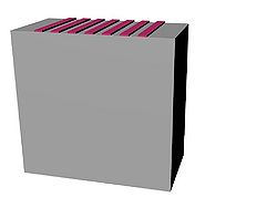 |
| 1.3 | Deep reactive ion etching (DRIE) | DRIE; Recipe: PolySOI10 Recipe needs to be tuned. Adjusted parameters: temperature, etching and passivation times. | DRIE Pegasus. | 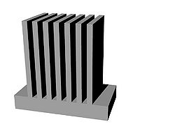 |
| 1.4 | Plasma surface treatment | To ensure that remainings of DUV resist are gone, samples are treated by O2/N2 plasma. (Optional step) | ||
| 1.5 | Scanning Electron Microscopy inspection | By cleaving the sample it is possible to inspect DRIE etched Si trenches in cross-sectional mode | 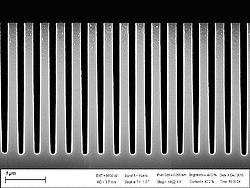 | |
| 1.6 | Atomic Layer Deposition of Al-doped ZnO (AZO) | Deposition carried at 200oC. Thickness is above 100 nm. | Equipment used: ALD Picosun R200. Standard recipe used: AZO 20T. | 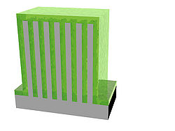 |
| 1.7 | Scanning Electron Microscopy inspection | By cleaving the sample it is possible to inspect ALD coatings deposited on Si trenches in cross-sectional mode | 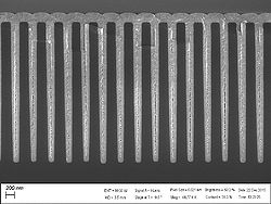 | |
| 1.8 | Ion Beam Etching (IBE). | Opening of deposited AZO top layer using recipe "Ti acceptance" there the stage was placed to 0o degree. The back side of the wafer also needs to be exposed to etching. | IBE/IBSD Ionfab 300 | 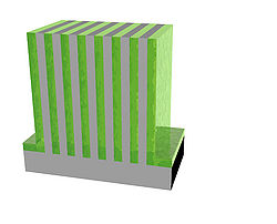 |
| 1.9 | Scanning Electron Microscopy inspection | By cleaving the sample it is possible to inspect IBE etching results in cross-sectional mode | 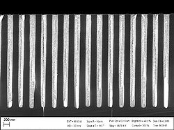 | |
| 1.10 | Selective etch of Si between ALD AZO coatings. | Si etching proceeds using reactive ion etching with isotropic process based on SF6 process gas. | Equipment used: RIE2. | 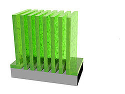 |
| 1.11 | Scanning Electron Microscopy inspection of fabricated structure. | Proof of final result. | 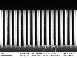 | |

