Specific Process Knowledge/Thin film deposition/MVD: Difference between revisions
Appearance
| Line 3: | Line 3: | ||
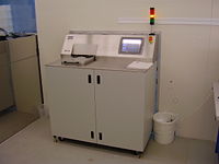
[[image:Mvd.jpg|200x200px|right|thumb|The MVD is located in cleanroom 1]] | [[image:Mvd.jpg|200x200px|right|thumb|The MVD is located in cleanroom 1]] | ||
The Applied Microstructures MVD 100 system deposits molecular films on surfaces. These films serve a wide range of purposes ranging from antistiction coatings of nanoimprint lithography stamps to protecting MEMS structures. | The Applied Microstructures MVD 100 system deposits molecular films on surfaces. These films serve a wide range of purposes ranging from antistiction coatings of nanoimprint lithography stamps to protecting MEMS structures. At Danchip the MVD is essential for nanoimprint lithography. | ||
== Processing on the MVD == | |||
The MVD coatings are created as self-assembled monolayers on a surface when a molecular vapor of chemials is present. These chemicals typically have a teflon-like tail consisting of -(CF<sub>2</sub>)<sub>x</sub>CF<sub>3</sub> and, in the other end, a reactive group -Si(Cl<sub>x</sub>)<sub>3-x</sub>. | |||
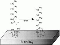
In most cases the chlorine atoms in the end of an flourinated organosilane react with -OH groups of the surface to form a chemical bond under elimination of HCL. | |||
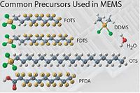
<gallery caption="Some chemicals of the MVD and the surface reaction" widths="200px" heights="150px" perrow="2"> | <gallery caption="Some chemicals of the MVD and the surface reaction" widths="200px" heights="150px" perrow="2"> | ||
Revision as of 17:05, 3 April 2008
The Molecular Vapor Deposition Tool

The Applied Microstructures MVD 100 system deposits molecular films on surfaces. These films serve a wide range of purposes ranging from antistiction coatings of nanoimprint lithography stamps to protecting MEMS structures. At Danchip the MVD is essential for nanoimprint lithography.
Processing on the MVD
The MVD coatings are created as self-assembled monolayers on a surface when a molecular vapor of chemials is present. These chemicals typically have a teflon-like tail consisting of -(CF2)xCF3 and, in the other end, a reactive group -Si(Clx)3-x.
In most cases the chlorine atoms in the end of an flourinated organosilane react with -OH groups of the surface to form a chemical bond under elimination of HCL.
- Some chemicals of the MVD and the surface reaction
-
Different chemicals for the MVD.
-
The chemical reaction in which the Cl atoms of the precursors are eliminated under formation of HCl.
| O2 plasma | Flow | 200 sccm |
|---|---|---|
| Power | 250 Watts | |
| Time | 300 seconds | |
| Chemical # 1 (vapor order 1) | Name | FDTS |
| Line no. | 3 | |
| Cycles | 4 | |
| Pressure | 0.500 Torr | |
| Chemical # 2 (vapor order 2) | Name | Water |
| Line no. | 1 | |
| Cycles | 1 | |
| Pressure | 18 Torr | |
| Processing | Time | 900 seconds |
| Purge | Cycles | 5 |


