Specific Process Knowledge/Etch/III-V ICP/GaN: Difference between revisions
Appearance
No edit summary |
|||
| Line 7: | Line 7: | ||
|'''Recipe''' | |'''Recipe''' | ||
|'''GaN Etch''' | |'''GaN Etch''' | ||
|'''GaN Etch for Si check''' | |||
|- | |- | ||
|Cl<sub>2</sub> flow | |Cl<sub>2</sub> flow | ||
|30 sccm | |30 sccm | ||
|27 sccm | |||
|- | |- | ||
|Ar flow | |Ar flow | ||
|10 sccm | |10 sccm | ||
|3 sccm | |||
|- | |||
|BCl3 flow | |||
|0 sccm | |||
|3 sccm | |||
|- | |- | ||
|Platen power | |Platen power | ||
|200 W | |200 W | ||
|75 W | |||
|- | |- | ||
|Coil power | |Coil power | ||
|600 W | |600 W | ||
|400 W | |||
|- | |- | ||
|Pressure | |Pressure | ||
|2 mTorr | |2 mTorr | ||
|4 mTorr | |||
|- | |- | ||
|Platen chiller temperature | |Platen chiller temperature | ||
|20 <sup>o</sup>C | |||
|20 <sup>o</sup>C | |20 <sup>o</sup>C | ||
|- | |- | ||
Revision as of 16:46, 17 January 2017
Feedback to this page: click here
GaN etching
| Recipe | GaN Etch | GaN Etch for Si check |
| Cl2 flow | 30 sccm | 27 sccm |
| Ar flow | 10 sccm | 3 sccm |
| BCl3 flow | 0 sccm | 3 sccm |
| Platen power | 200 W | 75 W |
| Coil power | 600 W | 400 W |
| Pressure | 2 mTorr | 4 mTorr |
| Platen chiller temperature | 20 oC | 20 oC |
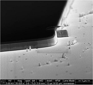
| Results (GaN Etch) | |
| GaN etch rate | 550-580 nm/min |
| SiO2 etch rate | 110-120 nm/min |
| Sidewall angle | ~ 90 o |
 |
|---|
