Specific Process Knowledge/Etch/III-V ICP/GaAsnano: Difference between revisions
Appearance
No edit summary |
No edit summary |
||
| Line 29: | Line 29: | ||
{| border="1" cellspacing="2" cellpadding="3" align="left" | {| border="1" cellspacing="2" cellpadding="3" align="left" | ||
|colspan="2" align="center"| '''Results (GaAs Nano Etch)''' | |colspan="2" align="center"| '''Results (GaAs Nano Etch)''' ''from 2011 by Thor Ansbæk @photonic'' | ||
|- | |- | ||
|GaAs | |GaAs | ||
Revision as of 08:53, 19 September 2016
Feedback to this page: click here
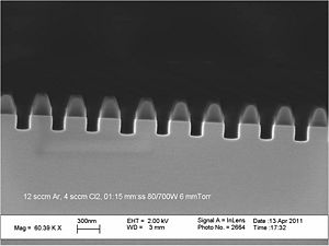
GaAs nano etch
| Recipe | GaAs Nano Etch |
| Cl2 flow | 4 sccm |
| Ar flow | 12 sccm |
| Platen power | 80 W |
| Coil power | 700 W |
| Pressure | 6 mTorr |
| Platen chiller temperature | 20 oC |
| Results (GaAs Nano Etch) from 2011 by Thor Ansbæk @photonic | |
| GaAs | 5 nm/s |
| AlInP | 1 nm/s |
| HSQ | 1.5 nm/s |
| ZEP520a | 2 nm/s |
| Si3N4 | 2 nm/s |
 |
|---|
