Specific Process Knowledge/Lithography/Pretreatment: Difference between revisions
No edit summary |
|||
| Line 113: | Line 113: | ||
* HMDS priming | * HMDS priming | ||
| | | | ||
* HMDS priming only | |||
|style="background:WhiteSmoke; color:black"| | |style="background:WhiteSmoke; color:black"| | ||
| Line 120: | Line 119: | ||
* HMDS priming and spin coating | * HMDS priming and spin coating | ||
| | | | ||
* HMDS priming only | |||
* HMDS priming and spin coating | |||
Revision as of 15:09, 12 August 2016
Feedback to this page: click here
Pretreatment
All surfaces can be divided to hydrophilic or hydrophobic surfaces. Oxidized surfaces such as SiO2 or surfaces with native oxide (e.g. Si or Al substrates) are considered to be hydrophilic and have very bad wetting with hydrophobic resist. The adhesion of most resists on hydrophilic surfaces is deteriorated if moisture is present on the surface.
Therefore it is very important to do the pretreatment step before the spinning. Here we will give an overview of treatments available at Danchip to promote photoresist adhesion.
Comparing pretreatment methods
| HMDS | Buffered HF-Clean | Oven 250C | |
|---|---|---|---|
| Generel description |
Vapor priming |
Native oxide strip |
Dehydration |
| Chemical |
hexamethyldisilazane (HMDS) |
12%HF with Ammoniumflouride |
none |
| Substrate size |
|
|
|
| Allowed materials |
Silicon, glass, and polymer substrates Film or pattern of all types |
|
|
| Restrictions | Type IV and resist/polymer on polymer substrate | Wafers with metal is not allowed | Resist is not allowed |
HMDS
Feedback to this section: click here
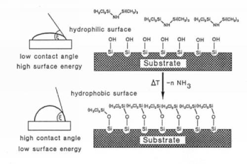
The chemical treatment with hexamethyldisilazane (HMDS) before the spin coating can be used to promote the adhesion for photoresist. Vapor priming with HMDS leaves a mono-layer of TMS (trimethylsilyl) on the Si or SiO2 surface. The process dehydrates the substrate surface, and lowers the surface tension.
The molecular formula for hexamethyldisilazane, or bis(trimethylsilyl)amine, is C6H19NSi2. Here is a schematic overview of HMDS treatment of silicon-oxide surface.

Comparing HMDS priming
| Equipment | HMDS oven | Oven: HMDS 2 | Spin Track 1 + 2 | Gamma UV | |
|---|---|---|---|---|---|
| Purpose |
|
|
|
| |
| Priming chemical |
hexamethyldisilizane (HMDS) | ||||
| Performance | Contact angle |
standard recipe 82° (on SiO2) |
60° - 90°; standard recipe 82° (on SiO2) |
||
| Process parameters | Process temperature |
150°C |
50°C |
||
| Process time |
32.5 minutes |
3 min / wafer |
|||
| Substrates | Substrate size |
|
100 mm wafers |
||
| Allowed materials |
Silicon, glass, and polymer substrates Film or pattern of all but Type IV and resist/polymer |
Silicon and glass wafers Film or pattern of all types |
|||
| Batch |
1 - 25, multiple batches possible |
1 - 25 |
|||
HMDS oven

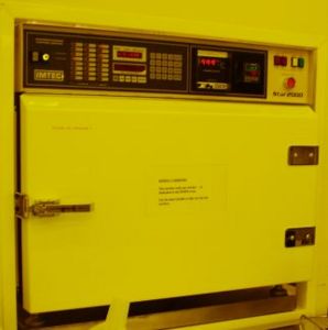
At Danchip we use Star2000 model from IMTEC to do vapor deposition of hexamethyldisilizane (HMDS) under the special conditions: low pressure and high chamber temperature. The result of the dehydration bake and HMDS prime is that the wafers become hydrophobic after the treatment.
The user manual, user APV, and contact information can be found in LabManager:
Process information
- Recipe 4: baseline prime process with 5 min priming time
Baseline prime process description:
1. Pump-down, 2 min
2. Nitrogen purge, 3.5 min
3. Heat-up, 10 min
4. Pump-down to 3 mBar
5. HMDS prime, 5 min
6. Chamber exhaust, 3 min
7. Nitrogen purge, 3.5 min
| Purpose |
Promotion of photoresist adhesion by hydrophobization | ||
|---|---|---|---|
| Chemical |
hexamethyldisilizane | ||
| Performance | Contact angle |
82° (on SiO2) | |
| Process parameters | Process temperature |
150 °C | |
| Process time |
32.5 minutes | ||
| Substrates | Substrate size |
| |
| Allowed materials |
Silicon, glass, and polymer substrates Film or pattern of all but Type IV and resist/polymer | ||
| Batch |
1 - 25, multiple batches possible | ||
Oven: HMDS 2
Comming soon.
The user manual, user APV, and contact information can be found in LabManager:
Process information
Buffered HF-Clean
Feedback to this section: click here

Another commonly used method to render the surface of silicon wafers hydrophobic is the dilute HF dip.
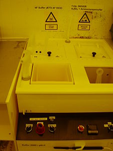
BHF is mostly used to do pretreatment step for new Si wafers. The native dioxide layer will be removed during 30 sec etching and in this way we will promote the resist adhesion on the Si substrates. We recommend to spin resist asap after the procedure.
The user manual, user APV, and contact information can be found in LabManager:
Buffered HF-Clean in LabManager
Process information
For more information on this BHF bath take a look here: Wet Silicon Oxide Etch (BHF)
Oven 250C
Feedback to this section: click here

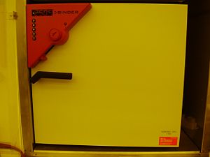
The oven is typically used for pretreatment (dehydration) of Si and glass substrates to promote the resist adhesion. We recommend to place the wafers in metal carrier in the oven at least for 4 hours, better during the night, and spin the resist on them asap.
The user manual, and contact information can be found in LabManager: Oven 250C
