Specific Process Knowledge/Characterization/SEM Supra 1: Difference between revisions
No edit summary |
|||
| Line 40: | Line 40: | ||
|style="background:LightGrey; color:black"|Imaging and measurement of | |style="background:LightGrey; color:black"|Imaging and measurement of | ||
|style="background:WhiteSmoke; color:black"| | |style="background:WhiteSmoke; color:black"| | ||
* | * Conducting samples | ||
* Semi-conducting samples | |||
* Thin (~ 5 µm <) layers of non-conducting materials such as polymers | |||
* Thick polymers, glass or quartz samples | |||
|- | |- | ||
!style="background:silver; color:black;" align="center" width="60"|Location | !style="background:silver; color:black;" align="center" width="60"|Location | ||
Revision as of 14:42, 4 May 2016
Feedback to this page: click here

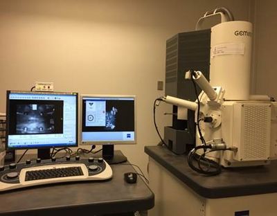
SEM Supra 1
The SEM Supra 1 a scanning electron microscope. It produces enlarged images of a variety of specimens, achieving magnifications of over 500.000x providing ultra high resolution imaging. This important and widely used analytical tool provides exceptional resolution and depth of field and requires minimal specimen preparation.
The SEM is a VP (variable pressure) instrument - Indicating that it is capable of operating at variable pressure. By increasing the pressure in the chamber it is possible to image isolating samples. The higher density of gas molecules will eliminate the charges at the cost of slightly reduced resolution. Also, the Se2 and InLens detectors will no longer work.
The SEM is the training SEM at DTU Danchip. It means that all new SEM users with no or little SEM experience must be trained on this tool and gain basic knowledge here before being qualified for training on other SEM's.
The SEM Supra 1 was installed in the cleanroom in November 2010, but it has now been relocated in the basement outside the cleanroom, so that users can avoid to clean samples that have been outside the cleanroom before SEM inspection.
The Balzer Sputter is located in the same room as the SEM Supra 1 and can be used to cover samples (for instance polymer samples from the Polymer Injection Molding tool) with a thin gold layer before SEM inspection to avoid charging problems.
Only users with samples that are somehow related to the cleanroom can use this SEM. Other users will have to contact DTU CEN.
The user manual, control instruction, the user APV and contact information can be found in LabManager:
SEM Supra 1 info page in LabManager,
Performance information
Equipment performance
| Equipment | SEM Supra 1 (Supra 40VP SEM) | |
|---|---|---|
| Purpose | Imaging and measurement of |
|
| Location |
| |
| Performance | Resolution |
The resolution is strongly dependent on the type of sample and the skills of the operator. |
| Instrument specifics | Detectors |
|
| Stage |
| |
| Electron source |
| |
| Operating pressures |
| |
| Options |
| |
| Substrates | Batch size |
|
| Allowed materials |
| |
