Specific Process Knowledge/Characterization/SEM: Scanning Electron Microscopy: Difference between revisions
| Line 300: | Line 300: | ||
|D | |D | ||
|E | |E | ||
|- | |||
|- | |||
|-style="background:LightGrey; color:black" | |||
!Options | |||
|CEN A | |||
|CEN B | |||
|CEN C | |||
|CEN D | |||
|CEN E | |||
|- | |- | ||
|- | |||
|-style="background:WhiteSmoke; color:black" | |||
!Stage specifications | |||
|A | |||
|B | |||
|C | |||
|D | |||
|E | |||
|- | |||
|- | |- | ||
|-style="background:LightGrey; color:black" | |-style="background:LightGrey; color:black" | ||
Revision as of 11:25, 19 April 2016
THIS PAGE IS UNDER CONSTRUCTION
Feedback to this page: click here


Scanning electron microscopy at Danchip
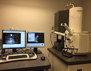
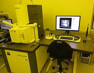
At Danchip there a four SEMs (scanning electron microscopes) that all cover a wide range of needs both in the cleanroom and outside: From the fast in-process verification of different process parameters such as etch rates, step coverages or lift-off quality to the ultra high resolution images on any type of sample intended for publication.
All four SEMs all manufactured by Carl Zeiss and have the same graphical user interface and very identical electron optics.
Three SEMs are located in the cleanroom (SEM Supra 2, SEM Supra 3 and SEM LEO), and one SEM is located in the basement (SEM Supra 1).
At the turn of the year 2015-2016 we made a reorganisation of the SEM's at Danchip. The old workhorse SEM's (the LEO and Supra 1) that have excellently served the users of the cleanroom for many years will be given new roles:
- The Leo SEM is a very reliable and rugged instrument that provides high quality images of most samples. It is exclusively dedicated to the users of the Raith E-beam lithography system so general imaging of user samples is no longer allowed.
- The SEM Supra 1 (formerly known as SEM Zeiss) has been relocated to the basement with two purposes: Serving the users that have samples from outside the cleanroom and serving as training tool; all new SEM users with no/little SEM experience must be trained on this tool and gain basic knowledge (typically 10 hours of usage) here before being qualified for training on other SEM's.
The two remaining SEM's at Danchip (called SEM Supra 2 and SEM Supra 3) serve as general imaging tools in the cleanroom. Like Supra 1, they are VP models from Carl Zeiss and will produce excellent images on any sample. The possibility of operating at higher chamber pressures in the VP mode makes imaging of bulk non-conducting samples possible. The SEM Supra 2 is also equipped with an airlock and an EDX detector.
The user manuals, quality control procedures and results, user APVs, technical information and contact information can be found in LabManager:
SEM's at DTU Danchip:
- The SEM Leo page in LabManager,
- The SEM Supra 1 page in LabManager,
- The SEM Supra 2 page in LabManager,
- The SEM Supra 3 page in LabManager,
Common challenges in scanning electron microscopy
| Equipment | SEM LEO | SEM Supra 1 | SEM Supra 2 | SEM Supra 3 | ||
|---|---|---|---|---|---|---|
| Purpose | Imaging and measurement of |
|
|
|
| |
| Instrument Position |
|
|
|
| ||
| Performance | Resolution | The resolution of a SEM is strongly dependent on the type of sample and the skills of the operator. The highest resolution is probably only achieved on special samples | ||||
|
|
|
| |||
| Instrument specifics | Detectors |
|
|
|
| |
| Stage |
|
|
|
| ||
| Electron source |
|
|
|
| ||
| Operating pressures |
|
|
|
| ||
| Options |
|
|
|
| ||
| Substrates | Sample sizes |
|
|
|
| |
| Allowed materials |
|
|
|
| ||
Comparison of the SEM's at CEN
| SEM Inspect S | SEM FEI Nova 600 NanoSEM | SEM FEI Quanta 200 ESEM FEG | FIB-SEM FEI QUANTA 200 3D | Dual Beam FEI Helios Nanolab 600 | |
|---|---|---|---|---|---|
| Purpose | A | B | C | D | E |
| Equipment position | CEN A | CEN B | CEN C | CEN D | CEN E |
| Instrument resolution | A | B | C | D | E |
| Detectors | CEN A | CEN B | CEN C | CEN D | CEN E |
| Stage specifications | A | B | C | D | E |
| Options | CEN A | CEN B | CEN C | CEN D | CEN E |
| Stage specifications | A | B | C | D | E |
| Substrate size |
|
| |||
| Allowed materials |
|
|
