Specific Process Knowledge/Back-end processing/Disco Saw: Difference between revisions
Appearance
| Line 86: | Line 86: | ||
|Leave 200 µm uncut. It's possible to cut through the sample. | |Leave 200 µm uncut. It's possible to cut through the sample. | ||
|-valign="top" | |-valign="top" | ||
|''' | |'''Max. sample thichness''' | ||
|not any limits | |not any limits | ||
|not any limits | |not any limits | ||
Revision as of 12:11, 27 February 2008
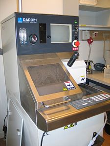
Disco Automatic dicing saw, model DAD321

The dicer feature versatile processing capabilities, compact designs, and high precision and reliability. Users perform workpiece loading, alignment, and unloading manually.
The dicer at DANCHIP is placed in room ?? on the first floor in bldg. 346. Please notice that this is not a cleanroom and that the dicingproces is very dirty. Think about how to clean your samples if you want to bring them back in the cleanroom.
A rough overview of the performance Disco DAD321 Dicer
| Purpose | Equipment for dicing out samples. |
|
|---|---|---|
| Performance | X-axis cutting range |
192 mm |
| . | . |
50 Å to 262 µm |
| . | Resolution xy |
down to 0.067 µm |
| . | Resolution z |
1Å, 10Å or 20Å |
| . | Max. scan depth as a function of trench width W |
1.2(W[µm]-5µm) |
| Hardware settings | Tip radius |
|
| Substrates | Substrate size |
|
| . | Substrate material allowed |
|
Comparing dicing parameters for different materials
| Silicon | Pyrex or bonded Si/Pyrex | |
|---|---|---|
| Bladetype | HUB Blade ZH05 (27HEEF) | HUBless Blade B1A862 |
| Cutlinewidth | 60 µm | 150 µm |
| Recommended feed speed | Up to 5 mm/sec | Up to 2 mm/sec |
| Recommended dice depth | Leave 200 µm uncut. It's possible to cut through the sample. | Leave 200 µm uncut. It's possible to cut through the sample. |
| Max. sample thichness | not any limits | not any limits |
| Index accuracy | not known | not known |
| Wavelength range | 400-1000 nm | 300-950 nm |
| What kind of thin films can be measured | Any film that is transparent to the light in the given wavelength range
ex:
|
Any film that is transparent to the light in the given wavelength range
ex:
|

