Specific Process Knowledge/Lithography/EBeamLithography/FilePreparation: Difference between revisions
| Line 461: | Line 461: | ||
RESIST 250 | RESIST 250 | ||
STDCUR 0.22 ;nA | STDCUR 0.22 ;nA | ||
END | |||
</pre> | |||
|- | |||
|} | |||
{| class="wikitable collapsible autocollapse" | |||
! Exposed patetrn aligned to global marks on a 4" wafer | |||
|- | |||
!colspan="2"| A 3*3 array of chips, each 1 mm*1 mm in size, is written on a 4” wafer, but only within a 3.8" diameter. The top left chip of the array (of patterns) is centered at (X,Y) = (-5000,35000). All chips are of pattern #1 detailed in the ‘mettekjan2012.v30’-file. A current of 0.88 nA is used in the dwell time calculation, and in the writing time estimation. A shot-shape modulation of 48 levels is applied to each chip. Before exposure, the calibration-path ‘DRF5M’ is applied. | |||
|- | |||
|- | |||
| | |||
SDF file | |||
<pre> | |||
MAGAZIN 'LAYERS' | |||
#1 | |||
%4A | |||
JDF 'berit',1 | |||
ACC 100 | |||
CALPRM '0.2na_ap5' | |||
GLMDET S | |||
CHIPAL 0 | |||
DEFMODE 2 | |||
OFFSET(0,0) | |||
END 1 | |||
</pre> | |||
JDF FILE | |||
<pre> | |||
JOB/W 'BERIT',4,3.8 | |||
PATH DRF5M | |||
ARRAY (-35000,3,1000)/(35000,3,1000) | |||
ASSIGN P(1)->((*,*),SHOT1) | |||
AEND | |||
PEND | |||
LAYER 1 | |||
P(1) 'mettekjan2012.v30' | |||
SPPRM 4.0,,,,1.0,1 | |||
STDCUR 0.88 ;nA | |||
SHOT1: MODULAT (( 0, -2.8 ) , ( 1, -2.0 ) , ( 2, -1.2 ) | |||
- , ( 3, -0.4 ) , ( 4, 0.5 ) , ( 5, 1.3 ) | |||
- , ( 6, 2.1 ) , ( 7, 3.0 ) , ( 8, 3.9 ) | |||
- , ( 9, 4.7 ) , ( 10, 5.6 ) , ( 11, 6.5 ) | |||
- , ( 12, 7.3 ) , ( 13, 8.2 ) , ( 14, 9.1 ) | |||
- , ( 15, 10.0 ) , ( 16, 11.0 ) , ( 17, 11.9 ) | |||
- , ( 18, 12.8 ) , ( 19, 13.7 ) , ( 20, 14.7 ) | |||
- , ( 21, 15.6 ) , ( 22, 16.6 ) , ( 23, 17.6 ) | |||
- , ( 24, 18.6 ) , ( 25, 19.5 ) , ( 26, 20.5 ) | |||
- , ( 27, 21.5 ) , ( 28, 22.5 ) , ( 29, 23.6 ) | |||
- , ( 30, 24.6 ) , ( 31, 25.6 ) , ( 32, 26.7 ) | |||
- , ( 33, 27.7 ) , ( 34, 28.8 ) , ( 35, 29.8 ) | |||
- , ( 36, 30.9 ) , ( 37, 32.0 ) , ( 38, 33.1 ) | |||
- , ( 39, 34.2 ) , ( 40, 35.3 ) , ( 41, 36.5 ) | |||
- , ( 42, 37.6 ) , ( 43, 38.7 ) , ( 44, 39.9 ) | |||
- , ( 45, 41.0 ) , ( 46, 42.2 ) , ( 47, 43.4 )) | |||
END | END | ||
Revision as of 11:25, 18 June 2015
Introduction

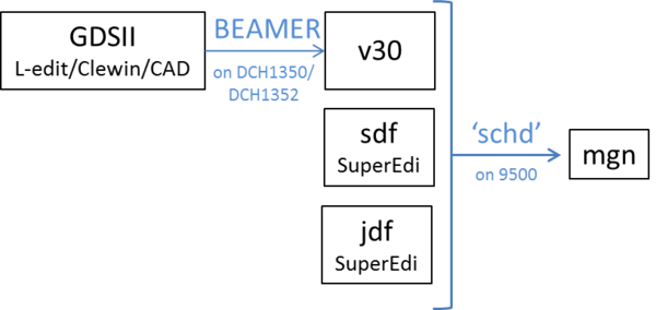
An e-beam exposure requires a v30-file, which contains information on the pattern to write, a jobdeck file (jdf-file), and a schedule file (sdf-file). The sdf- and jdf-file contain information about size and position of substrate, dose, current, and shot step. The sdf-file, jdf-file and v30-file are compiled to a magazine-file (mgn) on the 9500 computer.
When a magazine-file is prepared, the actual shot time can be estimated by the e-beam computer (9500).
Preparing a GDS file
If the layout is asymmetric, the conversion might result in an offset of the final layout onto the wafer. It is therefore recommended to symmetrise the layout, e.g. by inserting small structures in the corners of a rectangle that covers the layout.
How to convert to GDS in L-edit:
1 In L-edit, click File/Export Mask Data/GDSII
2 Choose Default GDSII unit: 1 database unit = 0.001 microns
Even though you do not export hidden layers or un-selected cells, unwanted layers might appear in the final GDSII file. Therefore, after conversion til GDSII, check your layout in a different layout viewer, e.g. CleWin (freeware), or BEAMER.
Converting from GDS to v30 (BEAMER)
The gds-file is converted to a v30-file by using the programme BEAMER. Please read the special BEAMER manual for a more advanced description of the BEAMER program.
- Open BEAMER.
- Drag the ‘Import’-module to the top-right window of Layout Beamer, open the gds-file to convert
- If the pattern has abutting polygons and even overlapping polygons which lead to double exposure, incorrect simulations etc., this can be fixed by running a ‘Heal’ program; drag the ‘HEAL’-module on top of the gds-file
- Drag the ‘Export’-module on top of the gds-file, export to the location ‘C:\1 gds files\name\date’. Export in JEOL52-format and change field-size to 1000µm x 1000 µm (under 'Advanced’). Click RUN on the Export-icon to execute the whole procedure
The gds-file is now converted to v30-format. In order to check the layout pattern double-click on the v30-module and and a VIEW LAYOUT window will open.
Preparing sdf and jdf files
Sdf- and jdf-files should not be created or edited in a regular notepad or wordpad program. Use only SuperEdi, which is freeware and available on the computers in the e-beam room. When you save a sdf- or jdf-file in SuperEdi, make sure to set the line endings to UNIX.
Both the sdf- and jdf-file should carry names using no capital letters.
You can find templates of sdf- and jdf-files in the folder home/eb0/jeoleb/job/templates on the 9500 computer.
Simple sdf and jdf files
sdf-file
The sdf-file contains a series of commands and parameters that specifies jdf filename, type
of cassette, shot pitch and condition file. It also specifies whether the pattern to be exposed requires alignment.
Below, an explanation of the template 'simple.sdf'. Note that semicolon outcomments the text:
___________________________________________________________________________
MAGAZIN    'SIMPLE1'          The magazine name is SIMPLE1; max. 20 capital letters

#6                            Cassette from slot no. 6 is used
%4A                           Wafer of 4" in position A is exposed
JDF     'simple',1            Layer block no. 1 of the jdf-file 'simple.jdf' is exposed
ACC 100                       Acceleration voltage of 100keV is used
CALPRM '0.2na_ap5'            The condition file 0.2na_ap5 is used
DEFMODE 2                     Both deflectors are used (default)
RESIST 240                    A dose of 240 µC/cm2 is used
SHOT A,8                      The shot step between individual beam shots is 4 nm
OFFSET(0,0)                   An offset of 0 µm is applied in both X and Y

END                           After exposure, the stage is left empty, i.e. the cassette is unloaded

___________________________________________________________________________
Note that the unit in the SHOT command is in 0.5nm, i.e. 'SHOT A,16' gives a shot pitch of 8nm. If the next user of the machine has loaded a cassette in slot #10 and you wish to load that cassette after exposure, you can finalize the sdf-file with 'END 10'.
jdf-file
The jdf-file contains a series of commands and parameters that specifies what pattern (v30-file) is to be written where on the sample. It also specifies what calibrations are to be performed during writing.
The jdf-file 'simple.jdf' could look like this:
___________________________________________________________________________
JOB/W  'SIMPLE',4                             4" wafer, jobname is 'SIMPLE', max. 20 capital letters

PATH DRF5M                                    The DRF5M calibration is used (see section 3.3)
    ARRAY   (0,3,2000)/(0,3,3000)             see note 1
        ASSIGN  P(1) -> (*,1)                 Pattern 1 is assigned to row 1-3 coloumn 1
        ASSIGN  P(2) -> (*,2-3)               Pattern 2 is assigned to row 1-3 coloumn 2-3
        SKIP (1,1)                            Nothing is assigned to chip (1,1)
    AEND                                      End-command to 'ARRAY'
PEND                                          End-command to 'PATH'

LAYER   1                                     Start of layer block 1
P(1)  'template1.v30'                         Pattern 1 defined in 'template1.v30'
P(2)  'template2.v30'                         Pattern 2 defined in 'template2.v30'
SPPRM 4.0,,,,1.0,1                            Beam parameters (default - see section 6.2)
STDCUR  0.22 ;nA                              Beam current (in nA) used for writing, see note 2

END                                           End of jdf-file
___________________________________________________________________________
Note 1: 9 chips are written, the upper left chip has center in (X,Y) = (0,0). The pitch between the chips is 2 mm in x-direction and 3 mm in y-direction.
Note 2: You should always add 10% to the current defined in 'STDCUR'; this ensures you work well below a scan speed of 100 MHz and thus gives room for a fluctuating current.
___________________________________________________________________________
Calibration during writing (PATH)
The inital and cyclic calibration before and during an e-beam run is defined in the jdf-file, e.g. by 'PATH DRF5M'.
Every time a jdf-file is called from a sdf-file, i.e. for every sequence defined in the sdf-file, the inital calibration specified in the jdf-file will be executed. Therefore, in order to save writing time, design your files so as to keep as few sequences in the sdf-file as possible.
There are a number of calibration programs to chose from, the DRF5M is recommended when no alignment is required and FT01 recommended if alignment is required:
auto calib file     calibrations
 DRF5M 	            INITIAL: HEIMAP, CURRNT, DRIFT
                    CYCLIC: CURRNT, DRIFT (every 5 minutes without interupting the writing of a field)
 FT01 	            INITIAL: CURRNT, DRIFT
                    CYCLIC: CURRNT, DRIFT (every 5 minutes without interupting the writing of a field)
 DTU5M 	            INITIAL: HEIMAP,CURRNT,INITBE,PDEFBE,SUBDEFBE
                    CYCLIC: CURRNT, DRIFT (every 5 minutes without interupting the writing of a field)
 HEI 	            INITIAL: HEIMAP
                    CYCLIC: CURRNT (every 10 minutes)
Alignment and global mark detection
Alignment of an e-beamed pattern to an existing pattern on wafer or chip (direct writing mode) requires at least two alignment marks, P and Q, preferably positioned in quadrant II and IV of the wafer or chip (the x-coordinate of the global mark Q must be equal to or larger than the x-coordinate of the global mark P).
Before loading the cassette into the e-beam writer, the wafer or chip should be pre-aligned using the optical pre-aligner setup in the e-beam room. A description of this procedure is included in the main manual of the e-beam writer.
HEIMAP is discarded in direct writing mode, it thus is important to insert height measurements, by the HSWITCH and CHIPAL V1 or CHIPAL V4 command in the sdf-file. The height of the substrate will in either case be measured by a laser beam with a spot size 0.94 mm x 0.08 mm on the substrate.
HSWITCH:
HSWITCH ON,OFF: machine focusses beam to the Height average between P and Q marks
HSWITCH OFF,ON: machine focusses beam to the height average of chip marks
HSWITCH ON,ON: machine focusses beam to the height average of chip marks. The chip mark height will overrule the P and Q mark height during exposure.
If HSWITCH is omitted, HSWITCH ON, ON is default
CHIPAL V1/V4:
The virtual CHIPAL command in the sdf-file, CHIPAL V1 or CHIPAL V4, can be used to measure the height of the substrate at well-defined positions on the substrate, thus correcting for height variations before pattern writing. To use this, HSWITCH should be set to 'HSWITCH OFF,ON' or 'HSWITCH OFF,ON'.
CHIPAL V1: machine measures height at chip mark M1 (machine does not scan the mark) and focusses beam to this height before exposing
CHIPAL V4: machine measures height at chip mark M1, M2, M3 and M4 (machine does not scan the marks) and focusses beam to the average height before exposing
_____________________________________________________________

MAGAZIN    'ALIGN'

#1                        Cassette from slot no. 1 is used
%4A                       Wafer of 4" in position A is exposed
JDF     'align',1         Layer block no. 1 of the jdf-file 'align.jdf' is exposed
ACC 100                   Acceleration voltage is 100keV
CALPRM '0.2na_ap5'        The condition file 0.2na_ap5 is used
DEFMODE 2                 Both deflectors are used (default)
GLMDET S                  Semi-automatic global mark detection is used
CHIPAL 0                  No chip-mark detection is used
HSWITCH OFF,ON            Height mesaurements at chip mark positions

RESIST 240                A dose of 240 µC/cm2 is used
SHOT A,8                  The shot step between individual beam shots is 4 nm
OFFSET(0,0)               An offset of 0 µm is applied in both X and Y

END 1                     After exposure, cassette no. 1 is left on stage
______________________________________________________________
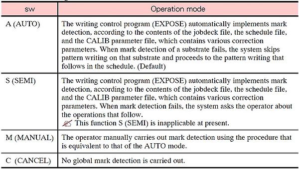
The parameters in the GLMDET-command can be as follows:
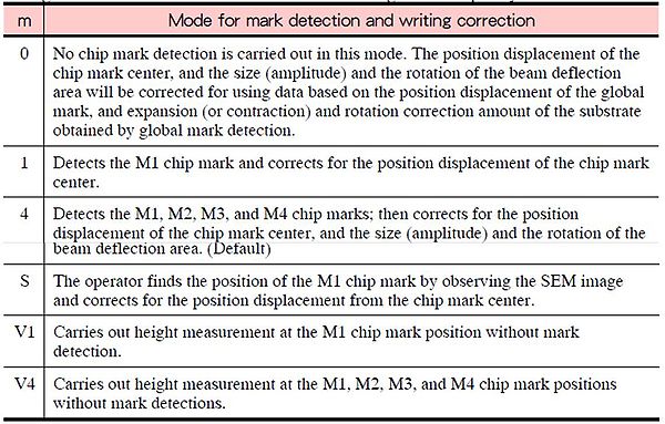
And the parameters in the CHIPAL-command can be as follows:
The global- and chip-mark position, size and orientation should be specified in the jdf-file:
______________________________________________________________
JOB/W  'ALIGN',4                           4" wafer, jobname is 'SIMPLE'

GLMPOS    P=(-7980,180),Q=(7960,-180)      Position of P and Q mark
GLMP      4.0,1000.0,t,f                   see note 1

PATH FT01                                  use FT01 when aligning, sec. 3.3
  ARRAY    (0,1,1000)/(0,1,1000)           1 chip starting in (0,0) is written

  CHMPOS M1=(-350,350),M2=(350,350),       Chipmark pos. in chip coordinate sys.
         M3=(350,-350),M4=(-350,-350)
     CHMARK 4.0,15.0, t, f                 see note 1

      ASSIGN  P(1) -> (*,*)                All chips are assigned to pattern 1

   AEND                                    End-command to 'ARRAY'
PEND                                       End-command to 'PATH'

LAYER   1                                  Layer 1 in the v30 file is written
P(1)  'align.v30'                          Pattern 1 defined in 'align.v30'
SPPRM 4.0,,,,1.0,1                         Beam parameters (see section 6.2)
STDCUR  0.22 ;nA                           Beam current (nA), se note 2.

END                                        End of jdf-file
_______________________________________________________________
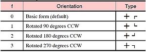
note 1: Width, length, type and orientation of global marks (GLMP) or chipmarks (CHMARK); the settings of the parameters t (type) and f (orientation) are listed in the two tables below:
note 2: Always add 10% to the current in this command to make sure you work well below 100 MHz and thus will not be affected if the current fluctuates above the base current.
Dose variation
The dose modulation is defined in a percentage addition to the base dose, i.e. the final dose, Q, is given by the base dose, RESIST, and modulation, m, by this formula:
Q = (RESIST · (100 + m))/100
In the jdf-file, you assign different layers of the pattern to different dose modulations, m.
If you define the dose variations by different datatype or layertype as described in section 3.2 of the BEAMER manual, you should define the dose for each layer number. You can check the layer numbers in BEAMER when you view the pattern, as seen in section 3.1 and 3.2 in the BEAMER manual.
JOB/W    'TINE1',4   ;4inch wafer

PATH   DRF5M
 ARRAY       (-500,1,1000)/(500,1,1000)
  ASSIGN P(1)->((*,*),SHOT1)
 AEND
PEND

LAYER  1
P(1)  'tinegjul122013a.v30'
SPPRM 4.0,,,,1.0,1
STDCUR  2.2 ;nA


SHOT1: MODULAT (( 0, -10) , ( 1, 0) , ( 2, 10))

END
The above example subtracts 10% from the base dose in layer 0 and adds 10% to the base dose in layer 2.
Alternatively, you can make simple dose variations by repeating a simple structure in an array in the jdf-file, and dedicate different part of the array to different doses:
JOB/W    'TINE1',4    ;4inch wafer


PATH   DRF5M
  ARRAY       (-1500,3,1000)/(1500,1,1000)
    ASSIGN P(1)->((1,1),SHOT1)
    ASSIGN P(1)->((2,1),SHOT2)
    ASSIGN P(1)->((3,1),SHOT3)
  AEND
PEND

LAYER  1

P(1)  'tinegjul122013b.v30'
SPPRM 4.0,,,,1.0,1
STDCUR  2.2 ;nA

SHOT1: MODULAT (( 0,-10))
SHOT2: MODULAT (( 0,0 ))
SHOT3: MODULAT (( 0,10))

END
Double current exposure
Before running a double-current exposure, you should receive training from a person from the e-beam staff. If this procedure is not performed correctly, it might end up in large pattern shifts.
A double-current exposure requires calibration of 2 condition files, of which you should calibrate the large current first and the small current afterwards. If the two patterns are aligned to each other, one should make sure the two condition files scan the same drift mark. The procedure is as follows:
- Load, restore and calibrate the condition file with the large current. When you scan the drift mark (using DRIFT), note the position of the drift mark (the position is written in the result display area of the calibration window).
- Increase the scan width in DRIFT to 40 µm in both X and Y. Save and execute DRIFT again.
- Save the condition file as usual.
- Load, restore and calibrate the condition file with the smallest current. When you scan the drift mark, make sure it scans the same mark as on the former condition file, i.e. that the two positions are equal within a few µm. If they are not, call a person from the e-beam team for help.
- Save the condition file as usual.
When you start the exposure, you call the condition file with the small current first. When the condition file with the large current is called, the state of the machine is restored to the condition file by the command 'RESTOR 1' in the sdf-file:
_____________________________________________________________
MAGAZIN    'DOUBLE'

#4
%4A
JDF     'smallcurrent',1
ACC 100
CALPRM '0.2na_ap5'
DEFMODE 2
RESIST 240
SHOT A,8
OFFSET(0,0)

#4
%4A
JDF     'largecurrent',1
ACC 100
CALPRM '10na_ap6'
DEFMODE 2
RESTOR 1                         Coloumn is restored to 10na_ap6 and lenses are demagnetized
RESIST 240
SHOT A,18
OFFSET(0,0)

END 4
______________________________________________________________
Using the 'RESTOR' command without '1' the condition file will be restored without demagnetizing of the lenses.
Compiling to mgn
Prepare jdf- and sdf-files according to the sections above.
Open FFFTP from the desktop of e.g. DCH1350 and connect to 9500. Move the jdf, adf and v30 files to the 9500 computer. The files should be located here before final compilation:
file type and its location (9500 computer)
sdf 	 home/eb0/jeoleb/job/danchip
jdf 	 home/eb0/jeoleb/job/danchip
v30 	 home/eb0/jeoleb/pattern/danchipv30
The sdf-file (with name 'sdfname.sdf'), the jdf-file (with name 'jdfname.jdf') and the v30-files are checked or compiled from a terminal from the location (DTU)/job/danchip with the following commands:
command
cmpl jdfname           Compiles the jdf-file alone, creates a lyr-file
schd sdfname           Final compilation of sdf, jdf and v30-files, creates a mgn-file
schd -exptim sdfname   Final compilation of sdf, jdf and v30-files, creates a mgn-files and states the writing time estimate
wrtestui               Opens a user interfaces wherefrom writing time etismation of a mgn-file can be estimated
After exposure, the sdf, jdf, and mgn-files are moved to this directory: home/eb0/jeoleb/job/danchipoldfiles.
A console may be opened by clicking Console in the Hosts tab (small triangle above 'cpu disk') in the tree at the bottom of the workspace. In the console, Ctrl + p or n may be used to browse through previous commands.
Checking the layout of the final mgn-file
The final check of pattern is performed clicking ‘Achk’ in the Analysis window:
- Open the mgn-file to inspect. Click on the pattern once (the pattern area turns red) and click ‘View/Shot Shape Display...’ to look at the actual pattern.
- Mark ‘Colored shot rank’ and ‘Fill in a pattern’ and select ‘ASD’ under ‘Shot form’. In order to see individual shots, zoom in and select a structure.
- Click the ‘Simulation ...’ button to select the correct Objective aperture. The simulated beam diameter will be displayed in the simulation window
Check that the pattern has not shifted in coordinates: In case it has, the pattern can be shifted back by manually changing the array-parameters in the jdf-file, or the SHIFT coordinates in the sdf-file
When the pattern is accepted by user, the e-beam exposure can start.
Examples
| 20 coloums of chips on a wafer; the first 10 coloums of the array is exposed with one shot pitch, the rest of the chips with another. | |
|---|---|
| An array of 20 chips is written on one 4" wafer. The first 10 coloums of the array is defined in layer block no. 1 of the jdf, coloumn 11-20 is defined in layer block no. 2 of the jdf. The two layer blocks uses different beam shot pitch and base dose. The two layer blocks must be called in two different sequences in the sdf-file. | |
|
SDF file MAGAZIN 'LAYERS' #1 %4A JDF 'layers',1 ACC 100 CALPRM '0.2na_ap5' DEFMODE 2 OFFSET(0,0) #1 %4A JDF 'layers',2 ACC 100 CALPRM '0.2na_ap5' DEFMODE 2 OFFSET(0,0) END 1 JDF FILE JOB/W 'TWOLAYERS',4
PATH DRF5M
ARRAY (-10000,20,2000)/( 10000,20,2000)
ASSIGN P(1) -> (1-10,*)
ASSIGN P(2) -> (11-20,*)
AEND
PEND
LAYER 1
P( 1 ) 'test2.v30'
SPPRM 4.0,,,,1.0,1
SHOT A,20
RESIST 220
STDCUR 0.22 ;nA
LAYER 2
P( 2 ) 'test2.v30'
SPPRM 4.0,,,,1.0,1
SHOT A,40
RESIST 250
STDCUR 0.22 ;nA
END
| |
| Exposed patetrn aligned to global marks on a 4" wafer | |
|---|---|
| A 3*3 array of chips, each 1 mm*1 mm in size, is written on a 4” wafer, but only within a 3.8" diameter. The top left chip of the array (of patterns) is centered at (X,Y) = (-5000,35000). All chips are of pattern #1 detailed in the ‘mettekjan2012.v30’-file. A current of 0.88 nA is used in the dwell time calculation, and in the writing time estimation. A shot-shape modulation of 48 levels is applied to each chip. Before exposure, the calibration-path ‘DRF5M’ is applied. | |
|
SDF file MAGAZIN 'LAYERS' #1 %4A JDF 'berit',1 ACC 100 CALPRM '0.2na_ap5' GLMDET S CHIPAL 0 DEFMODE 2 OFFSET(0,0) END 1 JDF FILE JOB/W 'BERIT',4,3.8 PATH DRF5M ARRAY (-35000,3,1000)/(35000,3,1000) ASSIGN P(1)->((*,*),SHOT1) AEND PEND LAYER 1 P(1) 'mettekjan2012.v30' SPPRM 4.0,,,,1.0,1 STDCUR 0.88 ;nA SHOT1: MODULAT (( 0, -2.8 ) , ( 1, -2.0 ) , ( 2, -1.2 ) - , ( 3, -0.4 ) , ( 4, 0.5 ) , ( 5, 1.3 ) - , ( 6, 2.1 ) , ( 7, 3.0 ) , ( 8, 3.9 ) - , ( 9, 4.7 ) , ( 10, 5.6 ) , ( 11, 6.5 ) - , ( 12, 7.3 ) , ( 13, 8.2 ) , ( 14, 9.1 ) - , ( 15, 10.0 ) , ( 16, 11.0 ) , ( 17, 11.9 ) - , ( 18, 12.8 ) , ( 19, 13.7 ) , ( 20, 14.7 ) - , ( 21, 15.6 ) , ( 22, 16.6 ) , ( 23, 17.6 ) - , ( 24, 18.6 ) , ( 25, 19.5 ) , ( 26, 20.5 ) - , ( 27, 21.5 ) , ( 28, 22.5 ) , ( 29, 23.6 ) - , ( 30, 24.6 ) , ( 31, 25.6 ) , ( 32, 26.7 ) - , ( 33, 27.7 ) , ( 34, 28.8 ) , ( 35, 29.8 ) - , ( 36, 30.9 ) , ( 37, 32.0 ) , ( 38, 33.1 ) - , ( 39, 34.2 ) , ( 40, 35.3 ) , ( 41, 36.5 ) - , ( 42, 37.6 ) , ( 43, 38.7 ) , ( 44, 39.9 ) - , ( 45, 41.0 ) , ( 46, 42.2 ) , ( 47, 43.4 )) END | |


