Specific Process Knowledge/Thin Film deposition/ALD/TiO2 deposition using ALD: Difference between revisions
No edit summary |
No edit summary |
||
| Line 3: | Line 3: | ||
'''Feedback to this page''': '''[mailto:labadviser@danchip.dtu.dk?Subject=Feed%20back%20from%20page%20http://labadviser.danchip.dtu.dk/index.php/Specific_Process_Knowledge/Thin_Film_deposition/ALD/TiO2_deposition_using_ALD click here]''' | '''Feedback to this page''': '''[mailto:labadviser@danchip.dtu.dk?Subject=Feed%20back%20from%20page%20http://labadviser.danchip.dtu.dk/index.php/Specific_Process_Knowledge/Thin_Film_deposition/ALD/TiO2_deposition_using_ALD click here]''' | ||
The ALD window for titanium dioxide (TiO<sub>2</sub>) ranges from 120 <sup>o</sup>C to 350 <sup>o</sup>C. | |||
A low temperatures between 120 <sup>o</sup>C and 150 <sup>o</sup>C an anatase TiO<sub>2</sub> layer is grow in the ALD, and at higher temperatures between 300 <sup>o</sup>C and 350 <sup>o</sup>C and amorphous TiO<sub>2</sub> layer is grown in the ALD. At temperatures between 150 <sup>o</sup>C and 300 <sup>o</sup>C the TiO<sub>2</sub> layer will be a mixture of both anatase and amorphous TiO<sub>2</sub>. | |||
SEM images of both anatase and amorphous TiO<sub>2</sub> are shown below. | |||
For Si wafers, anatase TiO<sub>2</sub> is best grown wafers without native oxide (do an BHF etch), and amorphous TiO<sub>2</sub> is best grown on wafers with native oxide. | |||
XPS measurements shows that at temperaturs below 120 <sup>o</sup>C the TiO<sub>2</sub> layer will be contaminated by Cl molecules from the TiCl<sub>4</sub> precursor. | |||
All results shown on this page have been obtained using the "TiO2" recipe on new Si(100) wafers with native oxide: | All results shown on this page have been obtained using the "TiO2" recipe on new Si(100) wafers with native oxide: | ||
Revision as of 11:59, 7 May 2015
THIS PAGE IS UNDER CONSTRUCTION

Feedback to this page: click here
The ALD window for titanium dioxide (TiO2) ranges from 120 oC to 350 oC.
A low temperatures between 120 oC and 150 oC an anatase TiO2 layer is grow in the ALD, and at higher temperatures between 300 oC and 350 oC and amorphous TiO2 layer is grown in the ALD. At temperatures between 150 oC and 300 oC the TiO2 layer will be a mixture of both anatase and amorphous TiO2.
SEM images of both anatase and amorphous TiO2 are shown below.
For Si wafers, anatase TiO2 is best grown wafers without native oxide (do an BHF etch), and amorphous TiO2 is best grown on wafers with native oxide.
XPS measurements shows that at temperaturs below 120 oC the TiO2 layer will be contaminated by Cl molecules from the TiCl4 precursor.
All results shown on this page have been obtained using the "TiO2" recipe on new Si(100) wafers with native oxide:
Recipe: TiO2
Temperature: 150 oC - 350 oC
| TMA | H2O | |
|---|---|---|
| Nitrogen flow | 150 sccm | 200 sccm |
| Pulse time | 0.1 s | 0.1 s |
| Purge time | 3.0 s | 4.0 s |
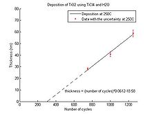
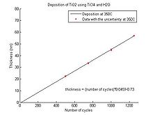
In the graphs below the TiO2 thickness as function of number of cycles for deposition temperatures between 150 oC and 350 oC can be seen. From the equations the number of cycles required for a certain thickess can be calculated.
- Titanium oxide thickness as function of number of cycles
-
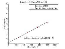 Temperature 150 oC.
 -
 Temperature 200 oC.
 -
 Temperature 250 oC.


