Specific Process Knowledge/Etch/KOH Etch: Difference between revisions
| Line 115: | Line 115: | ||
===Definition of <110> alignment structures=== | ===Definition of <110> alignment structures=== | ||
The etch rate dependence on the crystallographic planes can be used to determine the <110> crystal directions with high precision (better than +/- 0.05 | |||
Revision as of 19:31, 28 January 2008
KOH etch - Anisotropic silicon etch

KOH belongs to the family of anisotropic Si-etchants based on aqueous alkaline solutions. The anisotropy stems from the different etch rates in different crystal directions. The {111}-planes are almost inert whereas the etch rates of e.g. {100}- and {110}-planes are several orders of magnitude faster.
KOH-etching is a highly versatile and cheap way to realize micromechanical structures if you can live with the necessary SiN- or SiO masking materials and the K contamination of the surface. The latter necessitates in most cases a wet post-clean ('7-up' or RCA-clean) if the wafer is to be processed further.
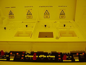
At Danchip we use as a standard a 28 wt% KOH. The etch rate - and the selectivity towards a SiO-mask - is depending on the temperature. We normally use T=80 oC but may choose to reduce this to e.g. 60 oC or 70 oC in case of a high-precission timed etch (e.g. defining a thin membrane). In some cases we recommend to saturate the standard 28 wt% KOH with IPA with an etch temperature at T=70 oC (reduce evaporation of IPA). One example is for boron etch-stop, where the selectivity towards the boron-doped silicon is improved compared to the standard etch. Key facts for the two solutions are resumed in the table:
KOH solutions
| 28 wt% KOH | 28 wt% KOH sat. with IPA | |
|---|---|---|
| General description |
Etch of Si(100) |
Etch of Si(100) with boron etch-stop |
| Chemical solution | KOH:HO 500 g : 1000 ml | KOH:HO:IPA 500 g : 1000 ml : ?? ml |
| Process temperature | 60 oC
70 oC 80 oC (standard - fast etch) |
70 oC
|
| Possible masking materials: | Stoichiometric SiN
Si-rich SiN PECVD SiN Thermal SiO |
Stoichiometric SiN Si-rich SiN PECVD SiN Thermal SiO
|
| Etch rate |
~0.4 µm/min (60 oC) ~0.7 µm/min (70 oC) ~1.3 µm/min (80 oC) |
~0.2 µm/min (70 oC) in p++ (doping level > 5x1019 cm-3) |
| Roughness |
Typical: 100-600 Å |
May form hillocks (pyramidal) |
| Batch size |
1-25 wafers at a time |
1-25 wafer at a time |
| Size of substrate |
4" wafers |
4" wafers |
| Allowed materials |
|
|
Definition of structures
Due to the almost inert (111)-planes
Definition of <110> alignment structures
The etch rate dependence on the crystallographic planes can be used to determine the <110> crystal directions with high precision (better than +/- 0.05
