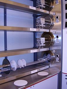
Specific Process Knowledge/Thermal Process/A4 Phosphor Pre-dep furnace: Difference between revisions
No edit summary |
No edit summary |
||
| Line 1: | Line 1: | ||
'''Feedback to this page''': '''[mailto:thinfilm@danchip.dtu.dk?Subject=Feed%20back%20from%20page%20http://labadviser.danchip.dtu.dk/index.php/Specific_Process_Knowledge/Thermal_Process/A4_Phosphor_Pre-dep_furnace click here]''' | '''Feedback to this page''': '''[mailto:thinfilm@danchip.dtu.dk?Subject=Feed%20back%20from%20page%20http://labadviser.danchip.dtu.dk/index.php/Specific_Process_Knowledge/Thermal_Process/A4_Phosphor_Pre-dep_furnace click here]''' | ||
[[Category: Equipment |Furnace]] | |||
[[Category: Thermal process|Furnace]] | |||
[[Category: Furnaces|A4]] | |||
==Phosphorus Pre-dep furnace (A4)== | ==Phosphorus Pre-dep furnace (A4)== | ||
Revision as of 14:29, 25 August 2014
Feedback to this page: click here
Phosphorus Pre-dep furnace (A4)

The Phosphorus Pre-dep furnace (A4) is used to dope Si wafers with phosphorus to make conductive structures, etch stop layers etc. The doping source is phosphoryl chloride (commonly called phosphorus oxychloride) which is a colourless liquid with the formula POCl3.
A4 is the lowest furnace tube in the A-stack positioned in cleanroom 2. The furnaces in the A-stack are the cleanest of all furnaces in the cleanroom. Please be aware of that all wafers have to be RCA cleaned before they enter the furnace, and check the cross contamination information in LabManager before you use the furnace.
The user manual, technical information and contact information can be found in LabManager:
Phosphorus Pre-dep furnace (A4)
Process knowledge
| Purpose |
|
|
|---|---|---|
| Process parameter range | Process Temperature |
|
| Process pressure |
| |
| Gasses on the system |
| |
| Substrates | Batch size |
|
| Substrate materials allowed |
|
