Specific Process Knowledge/Lithography/NanoImprintLithography: Difference between revisions
Appearance
| Line 1: | Line 1: | ||
==EVG NIL== | ==EVG NIL== | ||
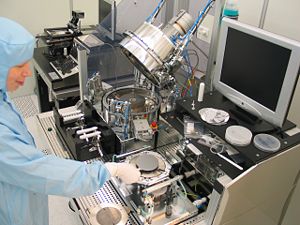
[[Image:EVG NIL.jpg| | [[Image:EVG NIL.jpg|300 × 300px|thumb|right|The EVG NIL is positioned in C-4]] | ||
'''Feedback to this section''': | '''Feedback to this section''': | ||
| Line 14: | Line 14: | ||
<br clear="all" /> | <br clear="all" /> | ||
==Process information== | ==Process information== | ||
====Types of Bonding==== | ====Types of Bonding==== | ||
Revision as of 17:17, 5 March 2014
EVG NIL

Feedback to this section: EVG NIL click here
The EVG NIL is a system for imprinting in polymers (Hot Embossing), and for bonding on wafer scale. 3 different types of bonding can be done: Anodic, Eutectic and Fusion. Furthermore it is possible to align the wafers one wishes to bond. In principle it is also possible to align the substrate and stamp before imprint, but it is much more difficult.
It is possible to fill bonded cavities with a desired gas. At the moment we have SF6 on the system, but if you would like another one, please contact Rune Christiansen.
The user manual, user APV, and contact information can be found in LabManager
Process information
Types of Bonding
Imprint information
| Purpose | Imprint and bonding |
|
|---|---|---|
| Performance | Alignment accuracy |
|
| Process parameter range | Process Temperature |
|
| Process pressure |
| |
| Piston Force |
| |
| Substrates | Batch size |
|
| Substrate material allowed |
| |
| Material allowed on the substrate |
|
