Specific Process Knowledge/Thin film deposition/MVD: Difference between revisions
Appearance
No edit summary |
No edit summary |
||
| Line 1: | Line 1: | ||
=<span style="background:#FF2800">THIS PAGE IS UNDER CONSTRUCTION</span>[[image:Under_construction.png|200px]]= | |||
'''Feedback to this page''': '''[mailto:photolith@danchip.dtu.dk?Subject=Feed%20back%20from%20page%20http://labadviser.danchip.dtu.dk/index.php/Specific_Process_Knowledge/Thin_film_deposition/MVD click here]''' | '''Feedback to this page''': '''[mailto:photolith@danchip.dtu.dk?Subject=Feed%20back%20from%20page%20http://labadviser.danchip.dtu.dk/index.php/Specific_Process_Knowledge/Thin_film_deposition/MVD click here]''' | ||
Revision as of 10:53, 20 January 2014
THIS PAGE IS UNDER CONSTRUCTION
Feedback to this page: click here
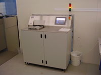
The Molecular Vapor Deposition tool

The Applied Microstructures MVD 100 system deposits molecular films on surfaces. These films serve a wide range of purposes ranging from antistiction coatings of nanoimprint lithography stamps to protecting MEMS structures. At Danchip the MVD is essential for nanoimprint lithography.
