Specific Process Knowledge/Characterization/Thickness Measurer: Difference between revisions
No edit summary |
|||
| Line 16: | Line 16: | ||
==Process knowledge== | ==Process knowledge== | ||
==Quality Control - Recipe Parameters and Limits== | |||
{| border="1" cellspacing="2" cellpadding="2" colspan="3" | |||
|bgcolor="#98FB98" |'''Quality Control (QC) for the Thickness measurer''' | |||
|- | |||
| | |||
*[http://www.labmanager.danchip.dtu.dk/d4Show.php?id=1831&mach=198 The QC procedure]<br> | |||
*[http://www.labmanager.danchip.dtu.dk/view_binary.php?fileId=2062 The newest QC data]<br> | |||
{| {{table}} | |||
| align="center" | | |||
{| border="1" cellspacing="1" cellpadding="2" align="center" style="width:200px" | |||
! QC Recipe: | |||
! Wet1050 | |||
! Dry1050 | |||
|- | |||
| H<sub>2</sub> flow | |||
|3 sccm | |||
|0 sccm | |||
|- | |||
|O<sub>2</sub> flow | |||
|2 sccm | |||
|5 sccm | |||
|- | |||
|Temperature | |||
|1050 C | |||
|1050 C | |||
|- | |||
|Oxidation time | |||
|30 min | |||
|100 min | |||
|- | |||
|} | |||
| align="center" valign="top"| | |||
{| border="2" cellspacing="1" cellpadding="2" align="center" style="width:500px" | |||
!QC limits | |||
|Thickness | |||
|Non-uniformity (both over a single wafer | |||
and over the boat) | |||
|- | |||
!Dry1050 | |||
|110-116 nm | |||
|3 % | |||
|- | |||
!Wet1050 | |||
|305-321 nm | |||
|5 % | |||
|- | |||
|} | |||
|- | |||
|} | |||
|} | |||
Revision as of 11:47, 13 January 2014
THIS PAGE IS UNDER CONSTRUCTION
Feedback to this page: click here
Thickness measurer
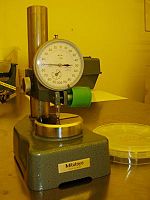
The purpose is to measure the thickness of wafers, depths of larger grooves or height of larger mesas.
Doing a KOH etch can it be helpful to insure no over etching by making a thickness measurement doing the etch.
The user manual, technical information and contact information can be found in LabManager:
Process knowledge
Quality Control - Recipe Parameters and Limits
| Quality Control (QC) for the Thickness measurer | ||||||||||||||||||||||||||
|
|
Purpose |
Measurer the thinkness of silicon wafer |
?? |
|---|---|---|
|
Performance |
?? |
?? |
|
Process parameter range |
Process Temperature |
|
| Process pressure |
| |
| Gasses on the system | ||
| Substrates | Batch size |
|
| Substrate materials allowed |
|
Feedback to this page: click here
This is a micrometer-screw.

It measures with an accurracy within a few µm. The range is from a few µm up to 5mm. Measure the wafer in the box next to the meter. If this is ok, then other wafers can be measured. There is a calibration device by the DEKTAK. It is calibrated at 750µm.
