Specific Process Knowledge/Characterization/AFM: Atomic Force Microscopy: Difference between revisions
| Line 15: | Line 15: | ||
|- | |- | ||
!style="background:silver; color:black;" align="left"|Purpose | !style="background:silver; color:black;" align="left"|Purpose | ||
|style="background:LightGrey; color:black"| | |style="background:LightGrey; color:black"|Topografic measurement in the nanometer and and sub-micron regime||style="background:WhiteSmoke; color:black"| | ||
* | *surface roughness measurement | ||
*step/structure hight measurement | |||
* | *Surface image | ||
*Surface | |||
|- | |- | ||
!style="background:silver; color:black" align="left"|Performance | !style="background:silver; color:black" align="left"|Performance | ||
|style="background:LightGrey; color:black"|Scan range xy||style="background:WhiteSmoke; color:black"| | |style="background:LightGrey; color:black"|Scan range xy||style="background:WhiteSmoke; color:black"| | ||
up to 90 µm square | |||
|- | |- | ||
|style="background:silver; color:black"|.||style="background:LightGrey; color:black"|Scan range z | |style="background:silver; color:black"|.||style="background:LightGrey; color:black"|Scan range z | ||
|style="background:WhiteSmoke; color:black"| | |style="background:WhiteSmoke; color:black"| | ||
1 µm (can go up to 6µm with special settings) | |||
|- | |- | ||
|style="background:silver; color:black"|.||style="background:LightGrey; color:black"|Resolution xy | |style="background:silver; color:black"|.||style="background:LightGrey; color:black"|Resolution xy | ||
|style="background:WhiteSmoke; color:black"| | |style="background:WhiteSmoke; color:black"| | ||
Down to 1.4 nm - accuracy better than 2% | |||
|- | |- | ||
|style="background:silver; color:black"|.||style="background:LightGrey; color:black"|Resolution z | |style="background:silver; color:black"|.||style="background:LightGrey; color:black"|Resolution z | ||
|style="background:WhiteSmoke; color:black"| | |style="background:WhiteSmoke; color:black"| | ||
<1 Å - accuracy better than 2% | |||
|- | |- | ||
|style="background:silver; color:black"|.||style="background:LightGrey; color:black"|Max. scan depth as a function of trench width W | |style="background:silver; color:black"|.||style="background:LightGrey; color:black"|Max. scan depth as a function of trench width W | ||
|style="background:WhiteSmoke; color:black"| | |style="background:WhiteSmoke; color:black"| | ||
1. | ~1 for our standard probe. Can be improved to about 10 with the right probe | ||
|- | |- | ||
!style="background:silver; color:black" align="left"|Hardware settings | !style="background:silver; color:black" align="left"|Hardware settings | ||
|style="background:LightGrey; color:black"|Tip radius | |style="background:LightGrey; color:black"|Tip radius of curvature | ||
|style="background:WhiteSmoke; color:black"| | |style="background:WhiteSmoke; color:black"| | ||
* | *Standrad probe: <12 nm | ||
|- | |- | ||
!style="background:silver; color:black" align="left"|Substrates | !style="background:silver; color:black" align="left"|Substrates | ||
|style="background:LightGrey; color:black"|Substrate size | |style="background:LightGrey; color:black"|Substrate size | ||
|style="background:WhiteSmoke; color:black"| | |style="background:WhiteSmoke; color:black"| | ||
*up to | *up to 6" | ||
|- | |- | ||
|style="background:silver; color:black"|.|| style="background:LightGrey; color:black"|Substrate material allowed | |style="background:silver; color:black"|.|| style="background:LightGrey; color:black"|Substrate material allowed | ||
Revision as of 15:24, 8 January 2008
Nanoman

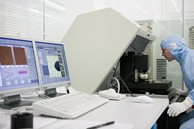
The AFM: Nanoman is a product of Veeco Instruments. AFM stands for Atomic Force Microscope which is a scanning probe microscope where a sharp probe is scanned across a surface either in contact mode or tapping mode. The outcome is a topographic plot of the surface. It has a lateral solution of about 1 nm and a vertical resolution of less than 1 Å which makes it very suitable for topographic characterization in the nanometer regime. The limiting factor however is often the size of the probe in use. The tip radius of curvature (ROC) can be from 2 nm up to more than 20 nm depending on the chosen probe. The half cone angle of the tip can vary from less than 3o to over 25o giving problems resolving high aspect ratio structures.
The main purposes are surface roughness measurements and step/structure high measurements in the nanometer and sub-micrometer regime. For larger structure see the topografic measurement page.
To get some product information from the vendor take a look at Veeco's homepage [1]
A rough overview of the performance of the AFM: Nanoman
| Purpose | Topografic measurement in the nanometer and and sub-micron regime |
|
|---|---|---|
| Performance | Scan range xy |
up to 90 µm square |
| . | Scan range z |
1 µm (can go up to 6µm with special settings) |
| . | Resolution xy |
Down to 1.4 nm - accuracy better than 2% |
| . | Resolution z |
<1 Å - accuracy better than 2% |
| . | Max. scan depth as a function of trench width W |
~1 for our standard probe. Can be improved to about 10 with the right probe |
| Hardware settings | Tip radius of curvature |
|
| Substrates | Substrate size |
|
| . | Substrate material allowed |
|
