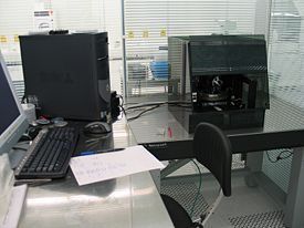
Specific Process Knowledge/Characterization/AFM: Atomic Force Microscopy: Difference between revisions
Appearance
| Line 8: | Line 8: | ||
<br clear="all" /> | <br clear="all" /> | ||
===A rough overview of the performance of | ===A rough overview of the performance of the AFM: Nanoman=== | ||
{| border="2" cellspacing="0" cellpadding="10" | {| border="2" cellspacing="0" cellpadding="10" | ||
Revision as of 12:39, 8 January 2008
Nanoman

The AFM: Nanoman is a product of Veeco Instruments.
To get some product information from the vendor take a look at Veeco's homepage [1]
A rough overview of the performance of the AFM: Nanoman
| Purpose | Profiler for measuring micro structures. |
|
|---|---|---|
| Performance | Scan range xy |
Line scan x: 50 µm to 200 mm |
| . | Scan range z |
50 Å to 262 µm |
| . | Resolution xy |
down to 0.067 µm |
| . | Resolution z |
1Å, 10Å or 20Å |
| . | Max. scan depth as a function of trench width W |
1.2(W[µm]-5µm) |
| Hardware settings | Tip radius |
|
| Substrates | Substrate size |
|
| . | Substrate material allowed |
|
