Specific Process Knowledge/Characterization/Profiler: Difference between revisions
No edit summary |
|||
| Line 13: | Line 13: | ||
|- | |- | ||
!style="background:silver; color:black;" align="left"|Purpose | !style="background:silver; color:black;" align="left"|Purpose | ||
|style="background:LightGrey; color:black"|Profiler for measuring micro structures | |style="background:LightGrey; color:black"|Profiler for measuring micro structures.||style="background:WhiteSmoke; color:black"| | ||
*Single point profiles | *Single point profiles | ||
*Wafer mapping | *Wafer mapping | ||
*Stress measurements by measuring wafer bow | *Stress measurements by measuring wafer bow | ||
*Surface roughness on a line scan | |||
|- | |- | ||
!style="background:silver; color:black" align="left"|Performance | !style="background:silver; color:black" align="left"|Performance | ||
|style="background:LightGrey; color:black"|Scan range xy||style="background:WhiteSmoke; color:black"| | |style="background:LightGrey; color:black"|Scan range xy||style="background:WhiteSmoke; color:black"| | ||
Line scan x: 50 µm to 200 mm | Line scan x: 50 µm to 200 mm | ||
|- | |- | ||
| Line 43: | Line 43: | ||
|style="background:LightGrey; color:black"|Tip radius | |style="background:LightGrey; color:black"|Tip radius | ||
|style="background:WhiteSmoke; color:black"| | |style="background:WhiteSmoke; color:black"| | ||
*5 µm | *5 µm 45<sup>o</sup> cone | ||
|- | |- | ||
!style="background:silver; color:black" align="left"|Substrates | !style="background:silver; color:black" align="left"|Substrates | ||
| Line 61: | Line 61: | ||
==Tencor stylus profiler== | ==Tencor stylus profiler== | ||
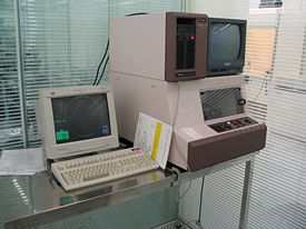
[[image:TencorP1.jpg|275x275px|right|thumb|Tencor: positioned in cleanroom 4 - glass cage no. 3]] | |||
Tencor P1 stylus profiler is a product of KLA-Tencor Corporation. It is usable for profiling surfaces of samples with structures in the micrometer range. It can measure in a specific point found with help from a high magnification video camera. It can also be used for stress measurements of thin films by measuring the wafer bow. | |||
It is a very old system and should be treated with care. | |||
<br clear="all" /> | |||
===A rough overview of the performance of Tencor P1 stylus profiler=== | |||
{| border="2" cellspacing="0" cellpadding="10" | |||
|- | |||
!style="background:silver; color:black;" align="left"|Purpose | |||
|style="background:LightGrey; color:black"|Profiler for measuring micro structures. ||style="background:WhiteSmoke; color:black"| | |||
*Single point profiles | |||
*Stress measurements by measuring wafer bow | |||
*Surface roughness on a line scan | |||
|- | |||
!style="background:silver; color:black" align="left"|Performance | |||
|style="background:LightGrey; color:black"|Scan range xy||style="background:WhiteSmoke; color:black"| | |||
Line scan x: Full substrate size | |||
|- | |||
|style="background:silver; color:black"|.||style="background:LightGrey; color:black"|Scan range z | |||
|style="background:WhiteSmoke; color:black"| | |||
<100 Å to ~0.3 mm | |||
|- | |||
|style="background:silver; color:black"|.||style="background:LightGrey; color:black"|Resolution xy | |||
|style="background:WhiteSmoke; color:black"| | |||
up to 5900 data points per profile | |||
|- | |||
|style="background:silver; color:black"|.||style="background:LightGrey; color:black"|Resolution z | |||
|style="background:WhiteSmoke; color:black"| | |||
1Å or 25Å | |||
|- | |||
|style="background:silver; color:black"|.||style="background:LightGrey; color:black"|Max. scan depth as a function of trench width W | |||
|style="background:WhiteSmoke; color:black"| | |||
0.87(W[µm]-5µm) | |||
|- | |||
|- | |||
!style="background:silver; color:black" align="left"|Hardware settings | |||
|style="background:LightGrey; color:black"|Tip radius | |||
|style="background:WhiteSmoke; color:black"| | |||
*5 µm 60<sup>o</sup> cone | |||
|- | |||
!style="background:silver; color:black" align="left"|Substrates | |||
|style="background:LightGrey; color:black"|Substrate size | |||
|style="background:WhiteSmoke; color:black"| | |||
*up to 4" | |||
|- | |||
|style="background:silver; color:black"|.|| style="background:LightGrey; color:black"|Substrate material allowed | |||
|style="background:WhiteSmoke; color:black"| | |||
*In principle all materials | |||
|- | |||
|} | |||
<br clear="all" /> | |||
==Comparing the profilers== | |||
Take a look at the [[Specific Process Knowledge/Characterization/Topographic measurement|topographic measurement]] page. | |||
Revision as of 11:32, 7 January 2008
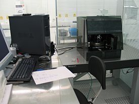
Dektak 8 stylus profiler

Dektak 8 stylus profiler is a product of Veeco Instruments. It is usable for profiling surfaces of samples with structures in the micrometer range. It can measure in a specific point found with help from high magnification video cameras or it can be programmed to measure several points defined with respect to some deskew points. It can also be used for stress measurements of thin films by measuring the wafer bow.
To get some product information and some tips and tricks from the vendor take a look at Veeco's homepage [1]
A rough overview of the performance of Dektak 8 stylus profiler
| Purpose | Profiler for measuring micro structures. |
|
|---|---|---|
| Performance | Scan range xy |
Line scan x: 50 µm to 200 mm |
| . | Scan range z |
50 Å to 262 µm |
| . | Resolution xy |
down to 0.067 µm |
| . | Resolution z |
1Å, 10Å or 20Å |
| . | Max. scan depth as a function of trench width W |
1.2(W[µm]-5µm) |
| Hardware settings | Tip radius |
|
| Substrates | Substrate size |
|
| . | Substrate material allowed |
|
Tencor stylus profiler

Tencor P1 stylus profiler is a product of KLA-Tencor Corporation. It is usable for profiling surfaces of samples with structures in the micrometer range. It can measure in a specific point found with help from a high magnification video camera. It can also be used for stress measurements of thin films by measuring the wafer bow.
It is a very old system and should be treated with care.
A rough overview of the performance of Tencor P1 stylus profiler
| Purpose | Profiler for measuring micro structures. |
|
|---|---|---|
| Performance | Scan range xy |
Line scan x: Full substrate size |
| . | Scan range z |
<100 Å to ~0.3 mm |
| . | Resolution xy |
up to 5900 data points per profile |
| . | Resolution z |
1Å or 25Å |
| . | Max. scan depth as a function of trench width W |
0.87(W[µm]-5µm) |
| Hardware settings | Tip radius |
|
| Substrates | Substrate size |
|
| . | Substrate material allowed |
|
Comparing the profilers
Take a look at the topographic measurement page.
