Specific Process Knowledge/Characterization/KLA-Tencor Surfscan 6420: Difference between revisions
Appearance
No edit summary |
|||
| Line 5: | Line 5: | ||
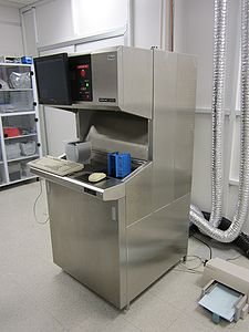
[[image:Surfscan_at_FAT.JPG|300x300px|right|thumb|The image is from the cleanroom at the place it was refurbish in California.]] | [[image:Surfscan_at_FAT.JPG|300x300px|right|thumb|The image is from the cleanroom at the place it was refurbish in California.]] | ||
Particle counting of an unpatterned surface. A broad range of particles size from 0. | Particle counting of an unpatterned surface. A broad range of particles size from 0.15 µm to greater than 3 µm can be measured on a polished silicon or epitaxial layers. Thin films like Nitride and thermal Oxide can also be inspected. The system will remove small surface roughness so it will not count as particles. | ||
Revision as of 09:18, 28 May 2013
Feedback to this page: click here
KLA-Tencor Surfscan 6420

Particle counting of an unpatterned surface. A broad range of particles size from 0.15 µm to greater than 3 µm can be measured on a polished silicon or epitaxial layers. Thin films like Nitride and thermal Oxide can also be inspected. The system will remove small surface roughness so it will not count as particles.
| Purpose |
| |
|---|---|---|
| Performance | Particles size |
|
| Througput |
| |
| Repeatbility |
| |
| Process parameter range | Process Temperature |
|
| Process pressure |
| |
| Substrates | Batch size |
|
| Substrate material allowed |
