Specific Process Knowledge/Thin film deposition/Electroplating-Ni: Difference between revisions
Appearance
No edit summary |
|||
| Line 11: | Line 11: | ||
<!-- remember to remove the type of documents that are not present --> | <!-- remember to remove the type of documents that are not present --> | ||
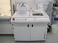
[[image: | [[image:choi_2017_Machine_overview.jpg|200x200px|right|thumb|Electroplating-Ni positioned in cleanroom 1]] | ||
<!-- give the link to the equipment info page in LabManager: --> | <!-- give the link to the equipment info page in LabManager: --> | ||
[http://labmanager.danchip.dtu.dk/function.php?module=Machine&view=view&mach= | [http://labmanager.danchip.dtu.dk/function.php?module=Machine&view=view&mach=274 LabManager] | ||
== Process information == | == Process information == | ||
Revision as of 14:31, 7 May 2013
THIS PAGE IS UNDER CONSTRUCTION
Feedback to this page: click here
Name of equipment
Write a short description of the equipment(s).
The user manual(s), quality control procedure(s) and results, user APV(s), technical information and contact information can be found in LabManager:

Process information
Link to process pages - e.g. one page for each material
Example:
- Etch of silicon using RIE
- Etch of silicon oxide using RIE
- Etch of silicon nitride using RIE
- Etch of photo resist using RIE
| Equipment | Equipment 1 | Equipment 2 | |
|---|---|---|---|
| Purpose |
|
| |
| Performance | Response 1 |
|
|
| Response 2 |
|
| |
| Process parameter range | Parameter 1 |
|
|
| Parameter 2 |
|
| |
| Substrates | Batch size |
|
|
| Allowed materials |
|
| |
