Specific Process Knowledge/Etch/Etching of Polymer: Difference between revisions
| Line 141: | Line 141: | ||
|-style="background:silver; color:black" | |-style="background:silver; color:black" | ||
! | ! | ||
![[Specific Process Knowledge/ | ![[Specific Process Knowledge/Etch/ASE (Advanced Silicon Etch)|ASE]] | ||
![[Specific Process Knowledge/ | ![[Specific Process Knowledge/Photolithography/Stripping equipment#Plasma_asher_1|Plasma asher 1]] | ||
![[Specific Process Knowledge/ | ![[Specific Process Knowledge/Photolithography/Stripping equipment#Plasma_asher_2|Plasma asher 2]] | ||
![[Specific Process Knowledge/ | ![[Specific Process Knowledge/Etch/RIE (Reactive Ion Etch)|RIE2]] | ||
![[Specific Process Knowledge/ | ![[Specific Process Knowledge/Etch/Wet Polymer Etch|By wet etch]] | ||
Revision as of 08:03, 9 April 2013
THIS PAGE IS UNDER CONSTRUCTION

Polymer dry etching
Upgrading the silicon etch capability at Danchip with the DRIE-Pegasus has pushed our old ASE (Advanced Silicon Etcher) out of the line so that it now only serves as backup silicon dry etcher. We have therefore decided that the ASE must be converted to a polymer etcher instead. Hence, it will join the plasma asher and to some extend the RIE's where polymer etching is allowed. In RIE1 it is only for removing photo resist before or after a RIE etch if the plasma asher cannot be used for some reason. On RIE2 you can get allowance for some other polymer etching but you have to ask first.
Etching of polymers on the ASE
SPTS has provided some recipes for polymer etching on the ASE. They have NOT been tested yet (As of August 2011) and we are therefore very interested in learning whatever experiences you have. Please contact Jonas. The recipes are located in the root folder. Please copy them to your own folder and modify them there for your own purposes as you would with any other recipe.
| Name | Materials | Process parameters | Comments by Kevin Riddell SPTS prior to any tests at Danchip | ||||||||
|---|---|---|---|---|---|---|---|---|---|---|---|
| Mask | Etched | O2 | CO2 | SF6 | He/Ar | Pressure | Temp | Coil | Platen | ||
| poly1 | Oxide hard mask | polyimide/PMMA | 0 | 50 | 0 | 0 | 4 | 0 | 600 | 150 | This will etch PMGI, PI, & standard resists. We've never tried it for PMMA, but it should work |
| poly2 | standard resists, PI PMMA | 20 | 0 | 0 | 20 | 3 | 10 | 600 | 150 | This will give higher etch rates & better selectivities, but slightly more bowed profiles | |
| poly3 | BCB | 43 | 0 | 7 | 0 | 4 | 20 | 800 | 150 | A good start point for PDMS / Ormocer-type Si/ inorganic-containing polymers. The SF6/O2 ratio will depend on the composition of the polymer. | |
CYTOP etching: Results by Fei Wang, DTU Nanotech
| Folder\name | Materials | Process parameters | Comments | ||||||||
|---|---|---|---|---|---|---|---|---|---|---|---|
| Mask | Etched | O2 | CO2 | SF6 | He/Ar | Pressure | Temp | Coil | Platen | ||
| set\microrea\feicy3 | 1.5 µm PR | CYTOP | 5 | 0 | 0 | 20 | 3 | 0 | 600 | 150 | Estimated etch rate ~1.3um/min, selectivity around 1:8, etch load app. 10% |
- The results of the CYTOP etching
-
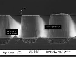 Profile
 -
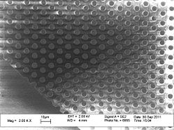 Top view
 -
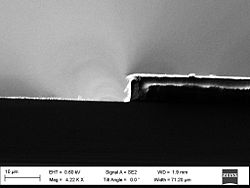 Profile


Feedback to this page: click here
Name of process
Write a short description of the process and how to perform the process.
Comparison method 1 and method 2 for the process
| ASE | Plasma asher 1 | Plasma asher 2 | RIE2 | By wet etch
| |
|---|---|---|---|---|---|
| Generel description | Generel description - method 1 | Generel description - method 2 | Generel description - method 3 | Generel description - method 4 | Generel description - method 5 |
| Parameter 1 |
|
|
|
|
|
| Parameter 2 |
|
|
|
|
|
| Substrate size |
|
|
|
|
|
| Allowed materials |
|
|
|
|
|