Specific Process Knowledge/Etch/IBE⁄IBSD Ionfab 300/IBE magnetic stack etch: Difference between revisions
Appearance
| Line 43: | Line 43: | ||
{| border="1" cellspacing="1" cellpadding="2" | {| border="1" cellspacing="1" cellpadding="2" | ||
! | ! | ||
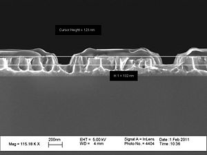
[[image:IBE | [[image:IBE magnetic stack A19-13.jpg|300x300px|thumb|center|Magnetic stack of Ta/MnIr/NiFe/Ta/Tao/Ta/MnIr/NiFe/Ta. Redeposition of etched material at photo resist. Profile 78°]] | ||
! | ! | ||
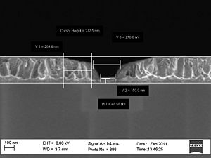
[[image:IBE acceptance Ti S10-5.jpg|300x300px|thumb|center|Ti s10-5: 270nm deep - 300nm line. All zep has gone. Profile: ~65 dg.]] | [[image:IBE acceptance Ti S10-5.jpg|300x300px|thumb|center|Ti s10-5: 270nm deep - 300nm line. All zep has gone. Profile: ~65 dg.]] | ||
Revision as of 13:26, 27 September 2012
End point detection is achieved by SIMS, and the etch rate is approximately 25 Nm/min. Resist stripping can be hard due to burned resist, to remedy this try to lover the current; this will though chance the sidewall angle. For help, discussion and further info please contact Kristian Hagsted Rasmussen.
Results from the acceptance test in February 2011
Process parameters for the acceptance test
| Parameter | Ti etch acceptance |
|---|---|
| Neutalizer current [mA] | 450 |
| RF Power [W] | 800 |
| Beam current [mA] | 400 |
| Beam voltage [V] | 500 |
| Beam accelerator voltage | 500 |
| Ar flow to neutralizer [sccm] | 5.0 |
| Ar flow to beam [sccm] | 10.0 |
| Rotation speed [rpm] | 20 |
| Stage angle [degrees] | 5 |
| Helium backside cooling [Torr] | 37.5 |


