Specific Process Knowledge/Etch/IBE⁄IBSD Ionfab 300/IBE Ti etch: Difference between revisions
Appearance
No edit summary |
No edit summary |
||
| Line 73: | Line 73: | ||
{| border="2" cellspacing="2" cellpadding="3" | {| border="2" cellspacing="2" cellpadding="3" | ||
!Parameter | !Parameter | ||
! | !Ti etch acceptance | ||
|- | |- | ||
|Neutalizer current [mA] | |Neutalizer current [mA] | ||
| Line 79: | Line 79: | ||
|- | |- | ||
|RF Power [W] | |RF Power [W] | ||
| | |1200 | ||
|- | |- | ||
|Beam current [mA] | |Beam current [mA] | ||
| Line 91: | Line 91: | ||
|- | |- | ||
|Ar flow to neutralizer [sccm] | |Ar flow to neutralizer [sccm] | ||
| | |6.0 | ||
|- | |- | ||
|Ar flow to beam [sccm] | |Ar flow to beam [sccm] | ||
| | |6.0 | ||
|- | |- | ||
|Rotation speed [rpm] | |Rotation speed [rpm] | ||
| Line 100: | Line 100: | ||
|- | |- | ||
|Stage angle [degrees] | |Stage angle [degrees] | ||
| | |20 | ||
|- | |- | ||
|} | |} | ||
| Line 107: | Line 107: | ||
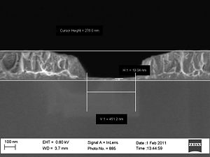
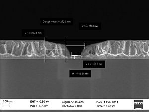
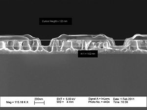
===Some SEM profile images of the etched | ===Some SEM profile images of the etched Ti=== | ||
{| border="1" cellspacing="1" cellpadding="2" | {| border="1" cellspacing="1" cellpadding="2" | ||
! | ! | ||
Revision as of 11:50, 5 January 2012
Results from the acceptance test in February 2011
Acceptance test for Ti etch:
| . | Acceptance Criteria |
Acceptance Results |
|---|---|---|
| Substrate information |
|
. |
| Material to be etched |
|
. |
| Mask information |
|
. |
| Features to be etched |
|
. |
| Etch depth |
|
|
| Etch rate |
|
|
| Etch rate uniformity |
|
|
| Reproducibility |
|
|
| Selectivity (Au etch rate/ZEP etch rate) |
|
|
| Etch profile |
|
|
Process parameters for the acceptance test
| Parameter | Ti etch acceptance |
|---|---|
| Neutalizer current [mA] | 550 |
| RF Power [W] | 1200 |
| Beam current [mA] | 500 |
| Beam voltage [V] | 600 |
| Beam accelerator voltage | 400 |
| Ar flow to neutralizer [sccm] | 6.0 |
| Ar flow to beam [sccm] | 6.0 |
| Rotation speed [rpm] | 20 |
| Stage angle [degrees] | 20 |


