Specific Process Knowledge/Characterization/Dektak 150: Difference between revisions
| Line 14: | Line 14: | ||
The user manual, technical information and contact information can be found in [http://labmanager.dtu.dk/function.php?module=Machine&view=view&mach=457 LabManager]. | |||
[http://labmanager.dtu.dk/function.php?module=Machine&view=view&mach=457 | |||
The computer is not connected to the network but data can be saved on a dedicated USB and transfered to a computer on the network. | The computer is not connected to the network but data can be saved on a dedicated USB and transfered to a computer on the network. | ||
Info about measurement accuracy can be found | Info about measurement accuracy can be found [//Dektak_XTA <b>here</b>] (''measured with Dektak XTA''). | ||
===Equipment performance and process related parameters=== | ===Equipment performance and process related parameters=== | ||
Revision as of 20:43, 27 May 2025
The content on this page, including all images and pictures, was created by DTU Nanolab staff, unless otherwise stated.
Feedback to this page: click here
Characterization Profiler
Profiler
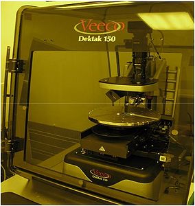
Stylus Profiler: Dektak150

The stylus profiler Dektak150 is intended for profile measurements on samples outside the cleanroom. The Dektak150 is especially well suited for measuring soft samples as it can be adjusted to apply lower force than the other stylus profilers at Nanolab.
The user manual, technical information and contact information can be found in LabManager.
The computer is not connected to the network but data can be saved on a dedicated USB and transfered to a computer on the network.
Info about measurement accuracy can be found here (measured with Dektak XTA).
| Purpose | Profiler for measuring micro structures| |
|
|---|---|---|
| Location | Building 347, room 080 |
|
| Performance | Scan range x y |
Line scan x: 50 µm to 55 mm in a single scan |
| Scan range z |
50 Å to 1 mm | |
| Resolution x y |
Theoretically down to 0.003 µm (in practice the resolution is limited by the tip size) | |
| Resolution z |
1Å (@65kÅ), 10Å (@655 kÅ), 80 Å (@5240 kÅ), 160 Å (@1mm) | |
| Maximum sample thickness |
100 mm | |
| Hardware settings | Tip radius |
|
| Substrates | Substrate size |
|
| Substrate materials allowed |
|
