
Specific Process Knowledge/Thin film deposition/ALD Picosun R200/ALD multilayers: Difference between revisions
mNo edit summary |
|||
| Line 193: | Line 193: | ||
<gallery caption="" widths=" | <gallery caption="" widths="400px" heights="350px" perrow="2"> | ||
image:TiO2_LT_Thickness.JPG| Measured thickness distribution across 100 mm wafer. | image:TiO2_LT_Thickness.JPG| Measured thickness distribution across 100 mm wafer. | ||
image:TiO2_LT_RI.JPG| Measured refractive index distribution across 100 mm wafer. | image:TiO2_LT_RI.JPG| Measured refractive index distribution across 100 mm wafer. | ||
Revision as of 19:05, 28 July 2025
The content on this page, including all images and pictures, was created by DTU Nanolab staff, unless otherwise stated.
Feedback to this page: click here
This page describes non-standart recipes including multilayers structures. They were the first test recipes on the ALD-1 to test the tool functionality and can be used as inspiration.
Low temperature deposition of Al2O3
Recipe: Al2O3 LT
Temperature: 80-150 oC
| TMA | H2O | |
|---|---|---|
| Nitrogen flow | 150 sccm | 200 sccm |
| Pulse time | 0.1 s | 0.2 s |
| Purge time | 5.0 s | 10.0 s |
Deposition rate: 0.089 nm/cycle (@120 oC)
This recipe has been developd for fabrication of high quality homogenious optical layers at low temperature. Research related results with this recipe can be found here: LINK - requires login (Phys. Rev. Lett. 115(17) 2015, 177402)
| Al2O3 deposition at 120 oC | |||||||||||||||||||||||||||||||
|
| |||||||||||||||||||||||||||||||
The uniformity, thickness, refractive index has been obtained using Ellipsometer VASE.
-
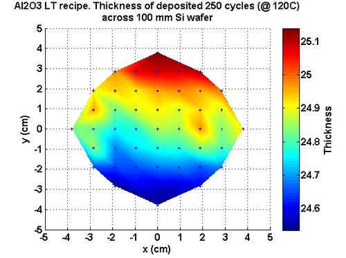 Measured thickness distribution across 100 mm wafer.
 -
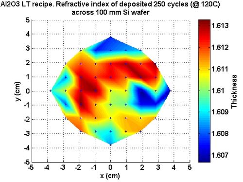 Measured refractive index distribution across 100 mm wafer.


Evgeniy Shkondin, DTU Nanolab, 2014-2016.
Low temperature deposition of TiO2
Recipe: TiO2 LT
Temperature: 80-150 oC
| TiCl4 | H2O | |
|---|---|---|
| Nitrogen flow | 150 sccm | 200 sccm |
| Pulse time | 0.2 s | 0.2 s |
| Purge time | 10.0 s | 15.0 s |
Deposition rate: 0.048 nm/cycle (@ 120 oC)
This recipe has been developd for fabrication of high quality homogenious optical layers at low temperature. The deposited TiO2 layers are amorphous. Research related results with this recipe can be found here: LINK - requires longin (Phys. Rev. Lett. 115(17) 2015, 177402)
| TiO2 deposition at 120 oC | |||||||||||||||||||||||||||||||
|
| |||||||||||||||||||||||||||||||
%%%%%%%%%%%%%%%%%%%%%%%%%%%%%%%%%%%%%%%%%%%%%%%%%%%%%%%%%%%%%%%
The uniformity, thickness, refractive index has been obtained using Ellipsometer VASE.
-
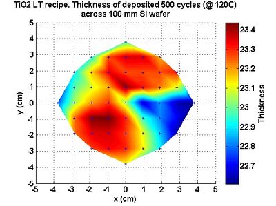 Measured thickness distribution across 100 mm wafer.
 -
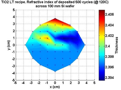 Measured refractive index distribution across 100 mm wafer.


Evgeniy Shkondin, DTU Nanolab, 2014-2016.
Low temperature grown multilayers on flat surfaces
Recipe: EMA01
Recipe: EMA02
Recipe: EMA03
Recipe: EMA04
Temperature: 120 oC
All four recipes is based on Al2O3_LT amd TiO2_LT above mentioned low temperature recipes. Optical research based on fabricated Al2O3 and TiO2 multilayers has been published LINK (Phys. Rev. Lett. 115(17) 2015, 177402)
-
 Al2O3/TiO2 multilayers.

Evgeniy Shkondin, DTU Nanolab (former DTU Danchip), 2014-2016.
Investigation of chemical composition in multilayers system
Chemical tace analysis has been performed using XPS K-Alpha equipment in depth profile mode.
-
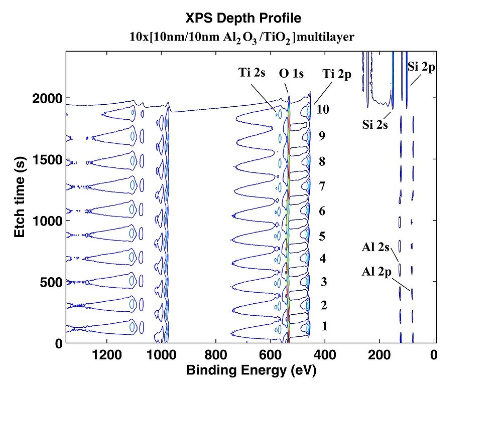 Survey scan.

-
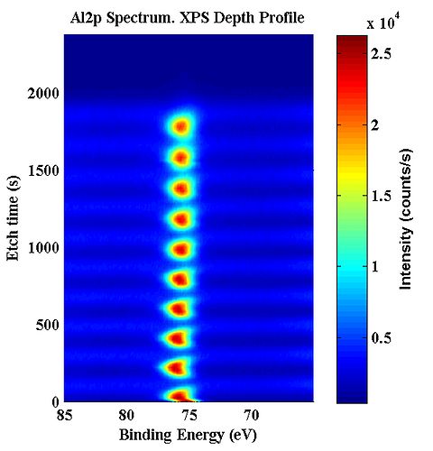 Al 2p signal multilayers.
 -
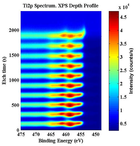 Ti 2p signal multilayers.
 -
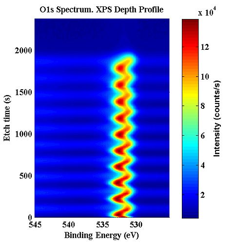 O 1s signal multilayers.
 -
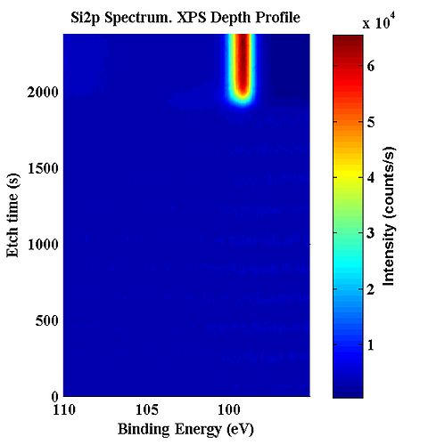 Si 2p signal multilayers.


Evgeniy Shkondin, DTU Nanolab (former DTU Danchip), 2014-2016.
Al2O3/TiO2 multilayers on high aspect ratio structures
Recipe: Multi T
Temperature: 150 oC
-
 Al2O3/TiO2 multilayers grown on silicon trenches.

Evgeniy Shkondin, DTU Nanolab (former DTU Danchip), 2014-2016.