Specific Process Knowledge/Lithography/EBeamLithography/AR-P 617: Difference between revisions
| Line 81: | Line 81: | ||
|- | |- | ||
| colspan="1" style="text-align: center;| | | colspan="1" style="text-align: center;| | ||
Bi-layer resist stack exposed at 400 µC/cm<sup>2</sup>. | Bi-layer resist stack exposed at 400 µC/cm<sup>2</sup>. Au coated for imaging. | ||
|} | |} | ||
Revision as of 09:44, 13 February 2024
AR-P 617 is a positive PMMA based E-beam resist from Allresist. Process information provided by Allresist can be found here.
Spin coating
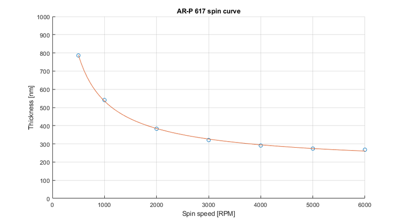
AR-P 617 can be spin coated on LabSpin 2 and 3 using the CSAR/PMMA bowlset. A spin curve for AR-P 617.06 is provided below. Process parameters are:
- Date: January 22nd 2024
- Coater: LabSpin 3
- Substrate: 2" Si
- Acceleration: 1000 RPM/s
- Time: 60 s
- Baking temperature: 200C (setpoint at 222C)
- Baking time: 120 s

|
|
AR-P 617.06 spin curve. |
Resulting resist thickness can be determined as y = axb+c, where y is thickness [nm], x is spin speed [RPM], a = 65274, b = -0.748 and c = 163.1.
Contrast curve
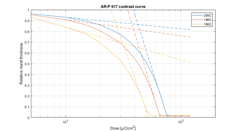
A contrast curve for AR-P 617.06 is provided below based on exposure at 100 kV for doses from 5 to 120 µC/cm2. The dose clear is dependent on softbake temperature, in this case 200C and 180C is used. Process parameters are:
- Date: February 5th 2024
- Coater: LabSpin 2
- Substrate: 2" Si
- Acceleration: 1000 RPM/s
- Time: 60 s
- Baking temperature: 200C, 180C and 160C
- Baking time: 120 s
- Exposure: 100 kV (JEOL 9500)
- Development: AR 600-50 for 90 seconds
- Stopper: IPA for 30 seconds + blow dry with nitrogen

|
|
AR-P 617.06 contrast curve from three different soft bake temperatures. Fitted lines are for determining contrast. |
Based on the fitted lines the contrasts are found to be 3.7, 4.2 and 4.3 for the 200C, 180C and 160 soft bake temperatures, respectively.
Development
AR-P is developed in AR 600-50 and IPA is used to rinse and stop development. As we have no dedicated setup for this it must be done in beakers in the EBL development fumehood in E4.
Typical development time is 60-90 seconds and it is recommended to rinse for 30 seconds in IPA.
Results
Dual layer for lift off
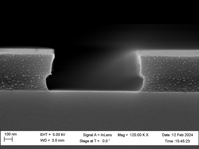
AR-P 617 can be used together with AR-P 6200 (CSAR) for a bi-layer lift-off friendly resist stack, where a slight undercut is made in the bottom layer. AR-P 617 has a higher sensitivity than AR-P 6200 and thus, if AR-P 617 is applied as the bottom layer, the higher sensitivity can lead to an undercut under the AR-P 6200 layer. The example below illustrates the process.
Bi-layer resist stack for lift off process:
- Date: February 12th 2024
- Substrate: 2" Si
- 1st layer coating
- Coater: Labspin 2
- RPM: 4000
- Spin time: 60 sec
- Acceleration: 1000 RPM/s
- Soft bake: 200C for 120 sec (setpoint at 222C)
- 2nd layer coating
- Coater: Gamma E-beam & UV
- Recipe: 2325-DCH 50mm CSAR 250nm
- Exposure tool: JEOL 9500 - 100 kV @ 29 nA
- 1st development
- Developer: EBL Manual
- Recipe: N50 90 sec
- 2nd development
- Manual development in fumehood 10 - AR 600-50 for 90 sec and 30 sec IPA rinse
The second development can be further extended to promote additional undercut.

|
|
Bi-layer resist stack exposed at 400 µC/cm2. Au coated for imaging. |
