| Recipe settings
|
SEM gallery
|
- On 6" wafer
- Coil Power [W]:2500
- Platen Power [W]: 200
- Platen temperature [oC]: 20
- H2 flow [sccm]:25.6
- C4F8 flow [sccm]: 25.6
- He flow [sccm]:448.7
- Pressure:Fully open APC valve (8-9 mTorr)
- Electromagnetic coils (EM) 'outer coil' / 'inner coil':'2 A' / '30 A'
- PLEASE DO NOT RUN WITH THESE SETTINGS FOR MORE THAN 6 MIN
|
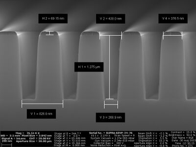
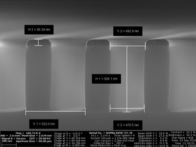
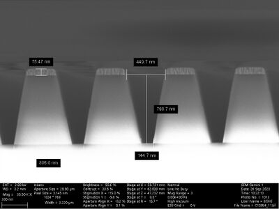
- SiO2 etch with Cr mask on full wafer 6 min etch
-
-
-
-
-
-
|
- Piece on Si carrier
- Coil Power [W]:2500
- Platen Power [W]: 200
- Platen temperature [oC]: 20
- H2 flow [sccm]:25.6
- C4F8 flow [sccm]: 25.6
- He flow [sccm]:448.7
- Pressure:Fully open APC valve (8-9 mTorr)
- Electromagnetic coils (EM) 'outer coil' / 'inner coil':'2 A' / '30 A'
- PLEASE DO NOT RUN WITH THESE SETTINGS FOR MORE THAN 6 MIN
|
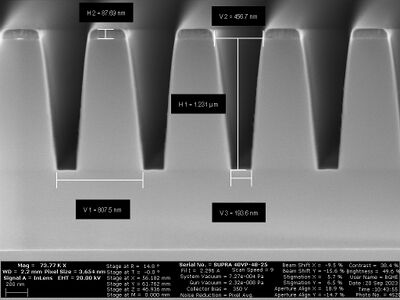
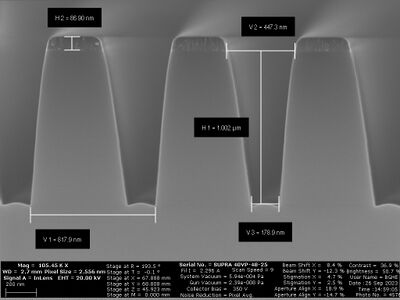
- SiO2 etch with Cr mask on wafer piece on Si carrier 6 min etch
-
-
-
-
-
-
|
- Coil Power [W]:2500
- Platen Power [W]: 200
- Platen temperature [oC]: 20
- H2 flow [sccm]:0
- C4F8 flow [sccm]: 25.6
- He flow [sccm]:448.7
- Pressure:Fully open APC valve (8-9 mTorr)
- Electromagnetic coils (EM) 'outer coil' / 'inner coil':'2 A' / '30 A'
- PLEASE DO NOT RUN WITH THESE SETTINGS FOR MORE THAN 6 MIN
|
- SiO2 etch with Cr mask on wafer piece on Si carrier 6 min etch, H2:0sccm
-
-
-
-
-
-
|
- Coil Power [W]:2500
- Platen Power [W]: 200
- Platen temperature [oC]: 20
- H2 flow [sccm]:0
- O2 flow [sccm]: 5
- C4F8 flow [sccm]: 25.6
- He flow [sccm]:448.7
- Pressure:Fully open APC valve (8-9 mTorr)
- Electromagnetic coils (EM) 'outer coil' / 'inner coil':'2 A' / '30 A'
- PLEASE DO NOT RUN WITH THESE SETTINGS FOR MORE THAN 6 MIN
|
- SiO2 etch with Cr mask on wafer piece on Si carrier 6 min etch, H2:0sccm, O2:5sccm
-
-
-
-
-
-
|
- Coil Power [W]:2500
- Platen Power [W]: 200
- Platen temperature [oC]: 20
- H2 flow [sccm]:0
- O2 flow [sccm]: 0
- C4F8 flow [sccm]: 13.0
- He flow [sccm]:225
- Pressure:Fully open APC valve (3.35 mTorr)
- Electromagnetic coils (EM) 'outer coil' / 'inner coil':'2 A' / '30 A'
- PLEASE DO NOT RUN WITH THESE SETTINGS FOR MORE THAN 6 MIN
|
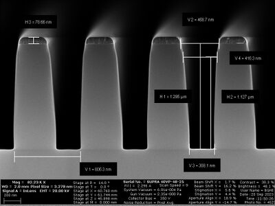
- SiO2 etch with Cr mask on wafer piece on Si carrier 6 min etch, H2:0sccm, C4F8:13sccm He:225sccm, Pressure:3.35mTorr
-
-
-
-
-
-
-
-
-
|
- Coil Power [W]:1200
- Platen Power [W]: 150
- Platen temperature [oC]: 20
- H2 flow [sccm]:0
- O2 flow [sccm]: 0
- C4F8 flow [sccm]: 13.0
- He flow [sccm]:225
- Pressure:Fully open APC valve (3.35 mTorr)
- Electromagnetic coils (EM) 'outer coil' / 'inner coil':'2 A' / '30 A'
- PLEASE DO NOT RUN WITH THESE SETTINGS FOR MORE THAN 6 MIN
|
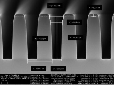
- SiO2 etch with Cr mask on wafer piece on Si carrier 6 min etch, H2:0sccm, C4F8:13sccm He:225sccm, Pressure:3.35mTorr; platen power 150W, coil power:1200W
-
-
-
-
-
-
|
- Coil Power [W]:1200
- Platen Power [W]: 150
- Platen temperature [oC]: 20
- H2 flow [sccm]:0
- O2 flow [sccm]: 10
- C4F8 flow [sccm]: 13.0
- He flow [sccm]:215
- Pressure:Fully open APC valve (3.35 mTorr)
- Electromagnetic coils (EM) 'outer coil' / 'inner coil':'2 A' / '30 A'
- PLEASE DO NOT RUN WITH THESE SETTINGS FOR MORE THAN 6 MIN
|
- SiO2 etch with Cr mask on wafer piece on Si carrier 6 min etch, H2:0sccm, C4F8:13sccm He:215sccm O2:10sccm, Pressure:3.6mTorr; platen power 150W, coil power:1200W
-
-
-
-
-
-
|
- Coil Power [W]:1200
- Platen Power [W]: 150
- Platen temperature [oC]: 20
- H2 flow [sccm]:0
- O2 flow [sccm]: 20
- C4F8 flow [sccm]: 13.0
- He flow [sccm]:205
- Pressure:Fully open APC valve (3.35 mTorr)
- Electromagnetic coils (EM) 'outer coil' / 'inner coil':'2 A' / '30 A'
- PLEASE DO NOT RUN WITH THESE SETTINGS FOR MORE THAN 6 MIN
|
- SiO2 etch with Cr mask on wafer piece on Si carrier 6 min etch, H2:0sccm, C4F8:13sccm He:205sccm O2:20sccm, Pressure:3.6mTorr; platen power 150W, coil power:1200W
-
-
-
-
-
-
-
|
- Coil Power [W]:1800
- Platen Power [W]: 150
- Platen temperature [oC]: 20
- H2 flow [sccm]:0
- O2 flow [sccm]: 10
- C4F8 flow [sccm]: 13.0
- He flow [sccm]:215
- Pressure:Fully open APC valve (3.35 mTorr)
- Electromagnetic coils (EM) 'outer coil' / 'inner coil':'2 A' / '30 A'
- PLEASE DO NOT RUN WITH THESE SETTINGS FOR MORE THAN 6 MIN
|
- SiO2 etch with Cr mask on wafer piece on Si carrier 6 min etch, H2:0sccm, C4F8:13sccm He:215sccm O2:10sccm, Pressure:3.6mTorr; platen power 150W, coil power:1800W
-
-
-
-
-
-
|
- Coil Power [W]:1800
- Platen Power [W]: 150
- Platen temperature [oC]: 20
- H2 flow [sccm]:0
- O2 flow [sccm]: 20
- C4F8 flow [sccm]: 13.0
- He flow [sccm]:205
- Pressure:Fully open APC valve (3.6 mTorr)
- Electromagnetic coils (EM) 'outer coil' / 'inner coil':'2 A' / '30 A'
- PLEASE DO NOT RUN WITH THESE SETTINGS FOR MORE THAN 6 MIN
|
|
- Coil Power [W]:1200
- Platen Power [W]: 100
- Platen temperature [oC]: 20
- H2 flow [sccm]:0
- O2 flow [sccm]: 20
- C4F8 flow [sccm]: 13.0
- He flow [sccm]:205
- Pressure:Fully open APC valve (3.6 mTorr)
- Electromagnetic coils (EM) 'outer coil' / 'inner coil':'2 A' / '30 A'
- PLEASE DO NOT RUN WITH THESE SETTINGS FOR MORE THAN 6 MIN
|
|
- Coil Power [W]:1800
- Platen Power [W]: 150
- Platen temperature [oC]: 20
- H2 flow [sccm]:0
- O2 flow [sccm]: 20
- C4F8 flow [sccm]: 13.0
- He flow [sccm]:205
- Pressure:Fully open APC valve (3.6 mTorr)
- Electromagnetic coils (EM) 'outer coil' / 'inner coil':'2 A' / '30 A'
- PLEASE DO NOT RUN WITH THESE SETTINGS FOR MORE THAN 6 MIN
|
- SiO2 etch with Cr mask on wafer piece on Si carrier 10 min etch, H2:0sccm, C4F8:13sccm He:205sccm O2:20sccm, Pressure:3.6mTorr; platen power 150W, coil power:1800W
-
-
-
-
-
-
-
-
|
- Coil Power [W]:1200
- Platen Power [W]: 100
- Platen temperature [oC]: 20
- H2 flow [sccm]:0
- O2 flow [sccm]: 20
- C4F8 flow [sccm]: 13.0
- He flow [sccm]:205
- Pressure:Fully open APC valve (3.9 mTorr)
- Electromagnetic coils (EM) 'outer coil' / 'inner coil':'0 A' / '0 A'
|
|
- Coil Power [W]:2500
- Platen Power [W]: 100
- Platen temperature [oC]: 20
- H2 flow [sccm]:0
- O2 flow [sccm]: 20
- C4F8 flow [sccm]: 13.0
- He flow [sccm]:205
- Pressure:Fully open APC valve (3.9 mTorr)
- Electromagnetic coils (EM) 'outer coil' / 'inner coil':'0 A' / '0 A'
|
- SiO2 etch with Cr mask on wafer piece on Si carrier 14 min etch, EM:0/0 H2:0sccm, C4F8:13sccm He:205sccm O2:20sccm, Pressure:3.9mTorr; platen power 100W, coil power:2500W
-
-
-
-
-
|
- Coil Power [W]:2500
- Platen Power [W]: 200
- Platen temperature [oC]: 20
- H2 flow [sccm]:0
- O2 flow [sccm]: 0
- C4F8 flow [sccm]: 13.0
- He flow [sccm]:225
- Pressure:Fully open APC valve (3.9 mTorr)
- Electromagnetic coils (EM) 'outer coil' / 'inner coil':'0 A' / '0 A'
|
- SiO2 etch with Cr mask on wafer piece on Si carrier 14 min etch, EM:0/0 H2:0sccm, C4F8:13sccm He:225sccm O2:0sccm, Pressure:3.9mTorr; platen power 200W, coil power:2500W
-
-
-
-
-
-
-
|
- 14 min
- Coil Power [W]:2500
- Platen Power [W]: 200
- Platen temperature [oC]: 20
- H2 flow [sccm]:0
- O2 flow [sccm]: 20
- C4F8 flow [sccm]: 13.0
- He flow [sccm]:205
- Pressure:Fully open APC valve (3.9 mTorr)
- Electromagnetic coils (EM) 'outer coil' / 'inner coil':'0 A' / '0 A'
|
- SiO2 etch with Cr mask on wafer piece on Si carrier 14 min etch, EM:0/0 H2:0sccm, C4F8:13sccm He:205sccm O2:20sccm, Pressure:3.9mTorr; platen power 200W, coil power:2500W
-
-
-
-
-
-
|
- Back to start setting without EM coils - 14 min
- Coil Power [W]:2500
- Platen Power [W]: 200
- Platen temperature [oC]: 20
- H2 flow [sccm]:25.6
- O2 flow [sccm]: 0
- C4F8 flow [sccm]: 25.6
- He flow [sccm]:448.7
- Pressure:Fully open APC valve (8-9 mTorr)
- Electromagnetic coils (EM) 'outer coil' / 'inner coil':'0 A' / '0 A'
|
- SiO2 etch with Cr mask on wafer piece on Si carrier 14 min etch, EM:0/0
-
-
-
-
-
-
-
-
-
|
- Coil Power [W]:600
- Platen Power [W]: 50
- Platen temperature [oC]: 20
- H2 flow [sccm]:0
- O2 flow [sccm]: 10
- C4F8 flow [sccm]: 6.5
- He flow [sccm]:100
- Pressure:Fully open APC valve (<2 mTorr)
- Electromagnetic coils (EM) 'outer coil' / 'inner coil':'0 A' / '0 A'
|
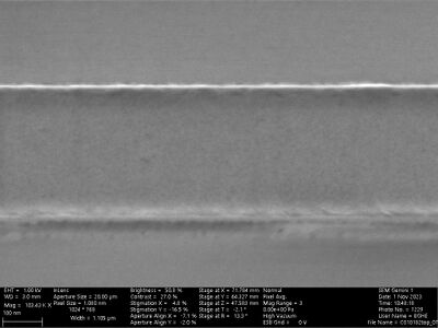
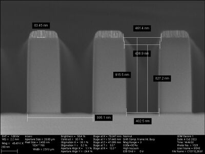
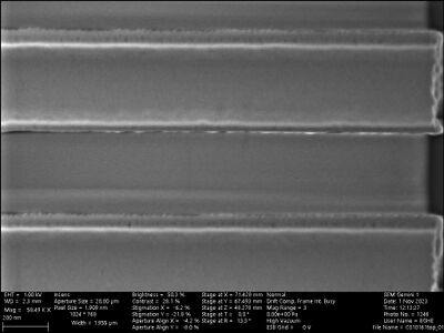
- C10751: SiO2 etch with Cr mask on wafer piece on Si carrier 20 min etch, EM:0/0 H2:0sccm, C4F8:6.5sccm He:100sccm O2:10sccm, Pressure:?mTorr; platen power 50W, coil power:600W
-
-
-
-
-
-
|
- Coil Power [W]:300
- Platen Power [W]: 25
- Platen temperature [oC]: 20
- H2 flow [sccm]:0
- O2 flow [sccm]: 10
- C4F8 flow [sccm]: 6.5
- He flow [sccm]:100
- Pressure:Fully open APC valve (<2 mTorr)
- Electromagnetic coils (EM) 'outer coil' / 'inner coil':'0 A' / '0 A'
|
- C10752: SiO2 etch with Cr mask on wafer piece on Si carrier 30 min etch, EM:0/0 H2:0sccm, C4F8:6.5sccm He:100sccm O2:10sccm, Pressure:?mTorr; platen power 25W, coil power:300W
-
-
-
-
-
-
|
- 45 min
- Coil Power [W]:300
- Platen Power [W]: 25
- Platen temperature [oC]: 20
- H2 flow [sccm]:0
- O2 flow [sccm]: 10
- C4F8 flow [sccm]: 6.5
- He flow [sccm]:100
- Pressure:Fully open APC valve (<2 mTorr)
- Electromagnetic coils (EM) 'outer coil' / 'inner coil':'0 A' / '0 A'
|
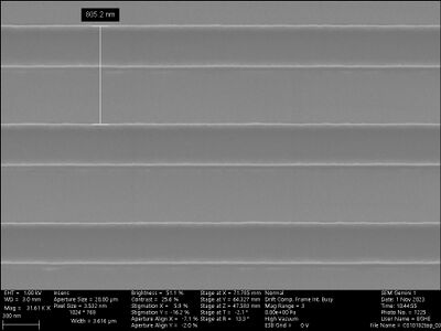
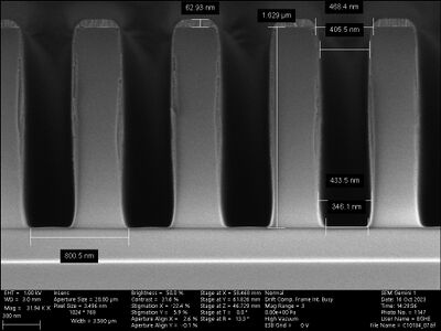
- C10834: SiO2 etch with Cr mask on wafer piece on Si carrier 45 min etch, EM:0/0 H2:0sccm, C4F8:6.5sccm He:100sccm O2:10sccm, Pressure:?mTorr; platen power 25W, coil power:300W
-
-
-
-
-
-
-
-
-
-
-
-
|
- Coil Power [W]:300
- Platen Power [W]: 20
- Platen temperature [oC]: 20
- H2 flow [sccm]:0
- O2 flow [sccm]: 10
- C4F8 flow [sccm]: 6.5
- He flow [sccm]:100
- Pressure:Fully open APC valve (<2 mTorr)
- Electromagnetic coils (EM) 'outer coil' / 'inner coil':'0 A' / '0 A'
|
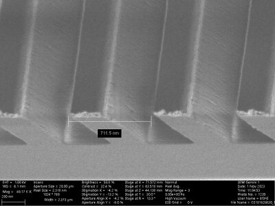
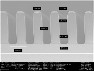
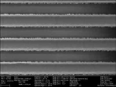
- C10844: SiO2 etch with Cr mask on wafer piece on Si carrier 50 min etch, EM:0/0 H2:0sccm, C4F8:6.5sccm He:100sccm O2:10sccm, Pressure:?mTorr; platen power 20W, coil power:300W
-
-
-
-
-
-
|


 pitch 800 nm
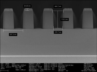 pitch 800 nm
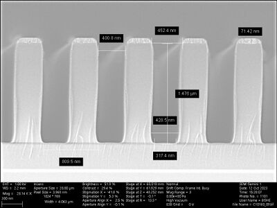
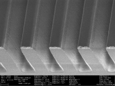
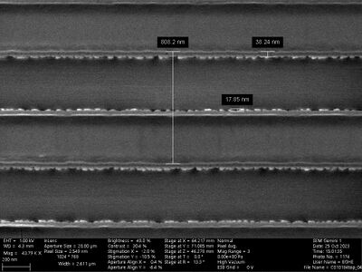
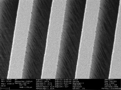 tilt 30 degrees
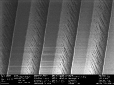 tilt 30 degrees
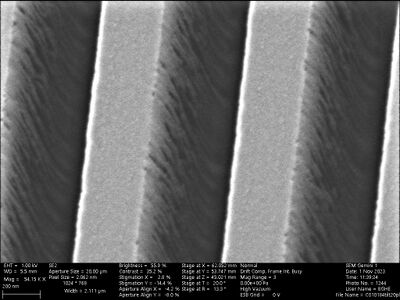 tilt 20 degrees
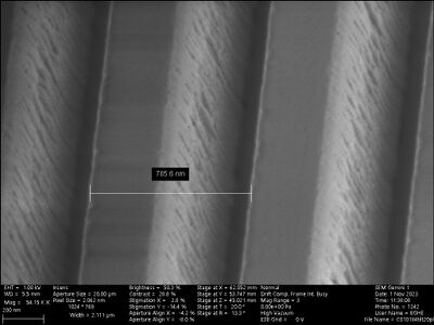 tilt 20 degrees