Specific Process Knowledge/Lithography/Descum: Difference between revisions
| Line 40: | Line 40: | ||
Descum of different resists, AZ5214E, AZ701 MiR and AZ2020 nLOF, on a single 100mm wafer was tested. Wafer was placed vertically in the middle of glass carrier. | Descum of different resists, AZ5214E, AZ701 MiR and AZ2020 nLOF, on a single 100mm wafer was tested. Wafer was placed vertically in the middle of glass carrier. | ||
Recipe setting was the same as in previous test in September 2019: 70ml/min O2, 70 ml/min N2, power 150W, different ashing time 1, 2, 3, 5 and 7 min run. Plasma Asher was cold before use, we observed minor temperature rise during processing, but not more than 5 degrees. Starting chambers pressure was around 0, 5 mbar. | Recipe setting was the same as in previous test in September 2019: 70ml/min O2, 70 ml/min N2, power 150W, different ashing time 1, 2, 3, 5 and 7 min run. Plasma Asher was cold before use, we observed minor temperature rise during processing, but not more than 5 degrees. Starting chambers pressure was around 0, 5 mbar. | ||
'''1,5 um AZ5214E resist''' | |||
{| {{table}} | |||
| align="center" | | |||
{| border="1" cellspacing="1" cellpadding="2" align="center" | |||
|- style="background:LightGrey" | |||
|'''Ashing time (min)'''|| 1|| 2 || 3 || 5 || 7 | |||
|- | |||
|'''Etched Thickness (nm)'''|| 6,28 || 102,99 || 76,92 || N/A || N/A | |||
|- | |||
|} | |||
|} | |||
'''1,5 um AZ5214E resist placed horizontally in the carrier''' | |||
{| {{table}} | |||
| align="center" | | |||
{| border="1" cellspacing="1" cellpadding="2" align="center" | |||
|- style="background:LightGrey" | |||
|'''Ashing time (min)'''|| 1|| 2 || 3 || 5 || 7 | |||
|- | |||
|'''Etched Thickness (nm)'''|| 63,03 || 143,32 || 304,29 || 372,59 || N/A | |||
|- | |||
|} | |||
|} | |||
'''1,5 um AZ701MiR resist''' | |||
{| {{table}} | |||
| align="center" | | |||
{| border="1" cellspacing="1" cellpadding="2" align="center" | |||
|- style="background:LightGrey" | |||
|'''Ashing time (min)'''|| 1|| 2 || 3 || 5 || 7 | |||
|- | |||
|'''Etched Thickness (nm)'''|| 6,28 || 102,99 || 76,92 || N/A || N/A | |||
|- | |||
|} | |||
|} | |||
'''1,5 um AZ 2020nLOF resist''' | |||
{| {{table}} | |||
| align="center" | | |||
{| border="1" cellspacing="1" cellpadding="2" align="center" | |||
|- style="background:LightGrey" | |||
|'''Ashing time (min)'''|| 1|| 2 || 3 || 5 || 7 | |||
|- | |||
|'''Etched Thickness (nm)'''|| 6,28 || 102,99 || 76,92 || N/A || N/A | |||
|- | |||
|} | |||
|} | |||
<br clear="all" /> | <br clear="all" /> | ||
===[http://labadviser.nanolab.dtu.dk/index.php/Specific_Process_Knowledge/Lithography/Strip#Plasma_Asher_2 Plasma asher 2]=== | ===[http://labadviser.nanolab.dtu.dk/index.php/Specific_Process_Knowledge/Lithography/Strip#Plasma_Asher_2 Plasma asher 2]=== | ||
Revision as of 11:12, 1 September 2021
Feedback to this page: click here
Descum results
Plasma asher 1

Descum of AZ5214E resist on 50mm silicon wafer. Wafer was placed horisontally in chamber on a 100 mm carier wafer.
Note: Plasma asher was cold before use
| ||||||||||||||||||||||||||||||||||||||||||||||||||
Conny Hjort & Jesper Hanberg September 2019
Descum of different resists, AZ5214E, AZ701 MiR and AZ2020 nLOF, on a single 100mm wafer was tested. Wafer was placed vertically in the middle of glass carrier. Recipe setting was the same as in previous test in September 2019: 70ml/min O2, 70 ml/min N2, power 150W, different ashing time 1, 2, 3, 5 and 7 min run. Plasma Asher was cold before use, we observed minor temperature rise during processing, but not more than 5 degrees. Starting chambers pressure was around 0, 5 mbar.
1,5 um AZ5214E resist
|
1,5 um AZ5214E resist placed horizontally in the carrier
|
1,5 um AZ701MiR resist
|
1,5 um AZ 2020nLOF resist
|
Plasma asher 2

Descum of AZ Mir 701 resist on 100mm silicon wafer. Five wafers were placed vertically in chamber.
Experiment parameters:
|
recipe 1
|

recipe 2
|
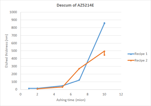
We can observe linear dependance of etched material on time after etching 7 minutes and more (recipe 2).
Jitka Urbánková & Jesper Hanberg
December 2019
