Specific Process Knowledge/Characterization/SEM LEO: Difference between revisions
| Line 7: | Line 7: | ||
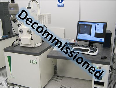
[[image:IMG_3290.jpg|400x400px|right|thumb|The SEM LEO located in cleanroom F-2]] | [[image:IMG_3290.jpg|400x400px|right|thumb|The SEM LEO located in cleanroom F-2]] | ||
The SEM LEO | The SEM LEO was a very reliable and rugged instrument that provided high quality SEM images of most samples and it served the users of the cleanroom for many years. Excellent images on a large variety of materials such as semiconductors, semiconductor oxides or nitrides, metals, thin films and some polymers were acquired by the thousands on the SEM. | ||
In her later years the SEM LEO was equipped with a Raith e-beam lithography system and was exclusively dedicated to the users of the Raith E-beam lithography. Decommissioned in early summer 2020, she is at DTU Mechanics. | |||
'''The user manual, control instruction and the user APV can still be found in LabManager:''' | |||
'''The user manual, control instruction | |||
[http://labmanager.dtu.dk/function.php?module=Machine&view=view&mach=37 SEM LEO info page in LabManager], | [http://labmanager.dtu.dk/function.php?module=Machine&view=view&mach=37 SEM LEO info page in LabManager], | ||
Revision as of 15:44, 16 November 2020
Feedback to this page: click here
The SEM LEO has been decommissioned and relocated to DTU Mechanics

The SEM LEO was a very reliable and rugged instrument that provided high quality SEM images of most samples and it served the users of the cleanroom for many years. Excellent images on a large variety of materials such as semiconductors, semiconductor oxides or nitrides, metals, thin films and some polymers were acquired by the thousands on the SEM.
In her later years the SEM LEO was equipped with a Raith e-beam lithography system and was exclusively dedicated to the users of the Raith E-beam lithography. Decommissioned in early summer 2020, she is at DTU Mechanics.
The user manual, control instruction and the user APV can still be found in LabManager:
SEM LEO info page in LabManager,
Performance information
Typical current values for EBL
Reported values are the average of five measurements from Elphy Quantum using the EBL holder's Faraday cup. All values in pA.
| LEO - Current measurements 11/02/2017 | |||||
| 5kV | 10kV | 15kV | 20kV | ||
|---|---|---|---|---|---|
| 10um | 13 | 17 | 20.5 | 25 | |
| 20um | 62 | 87 | 105 | 127 | |
| 30um | 160 | 175 | 215 | 264 | |
| 60um | 510 | 680 | 850 | 1040 | |
Equipment performance
| Equipment | SEM LEO (Leo 1550 SEM) | |
|---|---|---|
| Purpose | Imaging and measurement of |
|
| Other purpose |
| |
| Location |
| |
| Performance | Resolution |
The resolution is strongly dependent on the type of sample and the skills of the operator. |
| Instrument specifics | Detectors |
|
| Stage |
| |
| Electron source |
| |
| Operating pressures |
| |
| Options |
| |
| Substrates | Batch size |
|
| Allowed materials |
| |
