Specific Process Knowledge/Lithography/Aligners/Aligner: Maskless 02 processing: Difference between revisions
| Line 502: | Line 502: | ||
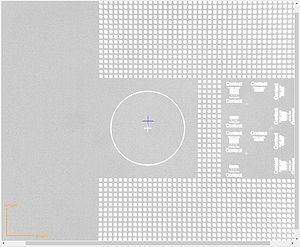
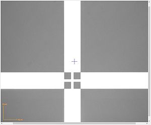
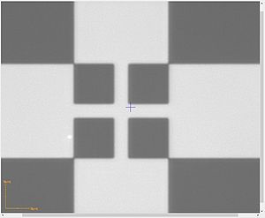
The results reported here use printed verniers to assess the misalignment along the two axes at different points on the wafer using an optical microscope. Two different designs were used; a ±5µm vernier and a ±1µm vernier. Both consist of a scale of 4µm lines with 10µm pitch, and a vernier scale to enable subdivision of the 5µm or 1µm scale into tenths, i.e. 0.5µm or 0.1µm. During inspection, observation of the symmetry of neighboring lines enables the observer to read the shifts with ±0.25µm or ±0.05µm accuracy. | The results reported here use printed verniers to assess the misalignment along the two axes at different points on the wafer using an optical microscope. Two different designs were used; a ±5µm vernier and a ±1µm vernier. Both consist of a scale of 4µm lines with 10µm pitch, and a vernier scale to enable subdivision of the 5µm or 1µm scale into tenths, i.e. 0.5µm or 0.1µm. During inspection, observation of the symmetry of neighboring lines enables the observer to read the shifts with ±0.25µm or ±0.05µm accuracy. | ||
The measurements are used to calculate the misalignment of the second layer with respect to the first print. The median of all measurement points in X or Y (reported as "Shift") is a measure for the average overall offset between the first and second print. At each point, this error is a combination of three contributions: The translational error ("Misplacement") is the amount by which the image is shifted; | The measurements are used to calculate the misalignment of the second layer with respect to the first print. The median of all measurement points in X or Y (reported as "Shift") is a measure for the average overall offset between the first and second print. At each point, this error is a combination of three contributions: The translational error ("Misplacement") is the amount by which the image is shifted; the run-in/run-out error ("Run-out") is the amount of gain in the image; and the rotational error ("Rotation") is the angle by which the image is rotated. The unit of ppm (parts per million) is used as rotation and run-out are generally small. A rotation of 1ppm corresponds to an angle of 0.2" (arcseconds) or a shift of 100nm across an entire 4" wafer, while a run-out of 1ppm corresponds to a shift of 50nm at the edge of a 4" wafer compared to the center. For comparison, the pixel size at the wafer surface is 160nm X 160nm, and the address grid size is 40nm. | ||
The deviations (±) given for the results here are calculated as half the range of measurements. If the range is smaller than the measurement uncertainty, the measurement uncertainty is used in stead. | The deviations (±) given for the results here are calculated as half the range of measurements. If the range is smaller than the measurement uncertainty, the measurement uncertainty is used in stead. | ||
The samples used for these tests are 100mm Si wafers coated with a 1.5µm layer of positive tone resist (AZ 5214E or MiR 701). | The samples used for these tests are 100mm Si wafers coated with a 1.5µm layer of positive tone resist (AZ 5214E or MiR 701). | ||
Revision as of 09:28, 14 April 2020
Feedback to this page: click here
Exposure technology
Aligner: Maskless 02 is not a direct writer. In the maskless aligner, the exposure light is passed through a spatial light modulator, much like in a video projector, and projected onto the substrate, thus exposing an area of the design at a time. The substrate is exposed by scanning the exposure field across the substrate in a succession of stripes.
The light source is a laser diode (array) with a wavelength of 375nm (2.8W) or 405nm (8W). The spacial light modulator is a digital micro-mirror device. The individual mirrors of the DMD are switched in order to represent the design, and the laser is flashed in order to yield the desired exposure dose. This image is projected onto the substrate through a lens(system). The projected image yields a pixel size of 160nm X 160nm at wafer scale. The image is scanned across the substrate, in order to expose the entire design, each stripe overlapping (2 or 4 times depending on exposure mode) in order to minimize uniformity effects and stitching errors. The address grid size is 80nm or 40nm for Fast or High Quality exposure mode, respectively.
The writing head of the Aligner: Maskless 02 moves only in the z-direction. Using an optical (or pneumatic) focusing system, the maskless aligner is able to do real-time autofocus. The defocus process parameter is used to compensate offsets in the focusing mechanism, and to optimize printing quality in different resists and varying thicknesses. The stage of the Aligner: Maskless 02 moves only in x and y. It has no theta-axis. All rotation during alignment is thus accomplished by transformation of the input design.
Process Parameters
The lithographic result of exposure on Aligner: Maskless 02 depends on a lot of factors, including the dose and defocus parameters, and the exposure mode used. The optimal dose and defocus depend on the type and thickness of the resist, and the optical properties of the substrate (e.g. reflective/absorbing/transparent). All of these factors influence the obtainable resolution, as well as the writing speed.
The correct way to determine the best dose-defocus settings is to generate a so-called Bossung plot (known from projection lithography), which plots the printed linewidth as a function of dose and defocus. From this, the most stable region of parameter space is chosen, i.e. the region where the linewidth changes the least when dose and defocus changes. Any deviation from the design linewidth may be corrected using the CD bias parameter. This typically involves SEM imaging of resist cross-sections, and quickly becomes time consuming. However, in most cases, inspection of a dose-defocus matrix (easily generated using the series exposure function) in an optical microscope will get you most of the way.
Data represent dose-defocus tests on Si using optical autofocus unless otherwise stated
| Thickness | Laser | Exposure mode | Dose | Defoc | Resolution | Comments | |
|---|---|---|---|---|---|---|---|
| AZ 5206E | 0.5 µm | 375 nm | Fast | 60 mJ/cm2 | -6 | 1 µm (not optimized) | Dev: 2xSP30s |
| Quality | 60 mJ/cm2 | -6 | ~750 nm (not optimized) | Dev: 2xSP30s | |||
| AZ 5214E | 1.5 µm | 405 nm | Fast | 90 mJ/cm2 | -2 | 1-2 µm | Dev: SP60s |
| 375 nm | Fast | 65 mJ/cm2 | 2 | ~1 µm | Dev: SP60s | ||
| Quality | 65 mJ/cm2 | 2 | ~750 nm | Dev: SP60s | |||
| AZ MiR 701 | 1.5 µm | 405 nm | Fast | 200 mJ/cm2 | -5 | ~1 µm (not optimized) | PEB: 60s@110°C, Dev: SP60s |
| 375 nm | Fast | 170 mJ/cm2 | -5 | 1 µm | PEB: 60s@110°C, Dev: SP60s | ||
| Quality | 180 mJ/cm2 | -6 (Feb 2019) -2 (Apr 2019) |
<750 nm | PEB: 60s@110°C, Dev: SP60s Large structures probably over-exposed | |||
| AZ nLOF 2020 | 2 µm | 375 nm | Fast | 400 mJ/cm2 | 5 | ~1 µm (not optimized) | PEB: 60s@110°C, Dev: SP60s Probably under-exposed |
| Quality | 400 mJ/cm2 | 0 | 1 µm | PEB: 60s@110°C, Dev: SP60s Probably under-exposed |
Exposure dose
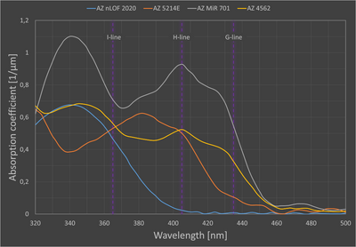
Exposure dose relative to exposure at 365nm (Aligner: Maskless 01):
| 375nm | 405nm | |
|---|---|---|
| AZ 5214E | 0.95 | 1.3 |
| AZ 4562 | ? | ? |
| AZ MiR 701 | 1 | 1.2 |
| AZ nLOF 2020 | 3 | NA |
| SU-8 | 10-15 | NA |
Defocus
The autofocus mode (optical or pneumatic) is selected via the substrate template.
Optical: Varies greatly with resist type and thickness, see Process Parameters. Probably also dependent on substrate. Should work for substrates down to 3x3mm2.
Pneumatic: Probably similar for resists of similar thickness, and not likely to vary with substrate. For 375nm exposure, the optimum seems to be around -15 to -10 (Large defocus range). Substrates must be at least 10x10mm2 to be successfully loaded, probably larger to successfully print.
Exposure mode
Aligner: Maskless 02 offers two exposure modes. The exposure mode is selected during design conversion.
High quality (4) mode is used for optimal resolution and minimum stripe stitching effects.
In the high quality mode, an area of the pattern is exposed by 4 stripes, each 160µm wide and exposing a quarter of the dose. At the same time, sub-pixel interpolation is applied, yielding an address grid size of 40nm.
Fast mode is used for maximum exposure speed.
In the fast mode, each area of the pattern is exposed by 2 stripes only. This effectively cuts the exposure time in half, but also doubles the size of the address grid in the X-direction. Due to less averaging of non-uniformities, stitching effects will be more prominent in this mode.
Writing speed
According to specs, the writing speed of Aligner: Maskless 02 is 285mm2/min in fast mode. Using the high quality exposure mode cuts this speed in half, to approximately 140mm2/min. The writing speed for a 100x100mm2 area measured during installation of the machine (acceptance test) was ~340mm2/min for both exposure wavelengths.
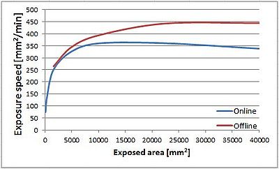
Speed vs. area:
During exposure of a stripe the stage moves at a constant speed. Each stripe thus includes a certain movement overhead for acceleration and deceleration. As the stripes get shorter, this overhead becomes more significant, and the normal writing speed is no longer achieved. For samples smaller than a 2" wafer, the writing speed of Aligner: Maskless 02 drops below the specified 285mm2/min.
When the exposure is started on the maskless aligner, the software starts converting the design to the data needed for the exposure. When sufficient data has been generated, the hardware starts exposing the sample while more data is being generated. This simultaneous data conversion and exposure is called Online conversion. Once a design has been converted (exposed) the data may be reused for repeated exposures (Offline conversion). Due to no time lost waiting for data, offline exposure may be several tens of % faster than online. However, the converted data can only be reused if no alignment is needed, including flat alignment ("Expose with substrate angle").
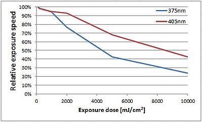
Speed vs. dose:
The writing speed remains almost constant up to a dose of 1000mJ/cm2. Due to the higher power of the 405nm laser, the writing speed remains high up to a dose of 2000mJ/cm2 for this wavelength. After this point, the writing speed decreases almost linearly with dose. For 375nm, the writing speed is 50% at a dose of 4500mJ/cm2, while 405nm requires a dose of 8500mJ/cm2 to drop to that speed.
Speed vs. design:
Depending on the complexity and density of the pattern, the conversion process may slow down the exposure significantly. A 4" wafer exposed with a pattern consisting of 200 million 5µm circles took 65 minutes (154mm2/min), compared to the specified 35 minutes (285mm2/min). It took 12 minutes before the first stripe was exposed.
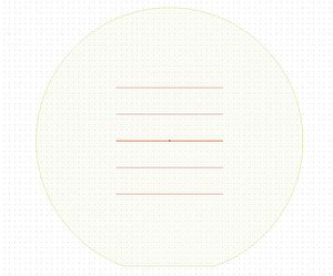
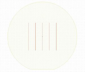
The maskless aligner exposes the design in north-south oriented stripes (perpendicular to the flat). The stripes all have the same length, set by the height of the design, and only completely empty stripes are skipped. The writing speed may thus be affected by the layout of the design, as shown below.
|
|
| This design printed in 6 minutes (260mm2/min) | This design printed in 1 minute (1600mm2/min) |
Acceptance test
Acceptance criteria on a 100 X 100 mm2 area: Width of smallest resolved line 600±100 nm, alignment error 500 nm, writing speed 285 mm2/min.
The acceptance test also included a verification of back side alignment (better than 1 µm), as well as functionality tests of grayscale and high aspect ratio mode.
Exposed on mask blank with 0.5 µm AZ1500 (possibly S1800) at DTU, then transferred via wet chrome etch and measured at Heidelberg
| SAT Feb 2019 | Width of smallest resolved line [nm] | Alignment error (TSA) [nm] | Exposure speed [mm2/min] | |
|---|---|---|---|---|
| 405 nm | X | 532±64 | 251 | 333 |
| Y | 599±58 | 382 | ||
| 375 nm | X | 556±44 | 214 | 347 |
| Y | 579±63 | 224 | ||
Features
Substrate centring and flat alignment
During substrate detection, the sample is scanned along the X- and Y-axes, as well as diagonally. From these measurements, the size (diameter) of the substrate is calculated, as well as the stage position matching the center of the substrate. This stage position will be the default origin for the subsequent exposure.
At the end of substrate detection, the sample is scanned twice along the bottom edge (flat), in order to determine the substrate rotation. This angle will be presented in the exposure panel along with the option to expose the design rotated in order to compensate for this angle, i.e. aligned to the flat/edge of the substrate.
Result of using "Expose with substrate angle" on three samples with optical autofocus:
- Rotation: 0.5±0.2°
- Centring:
- X 100±250µm
- Y 200±250µm
The error on the flat alignment is surprising when compared to the 0±0.1° measured on Aligner: Maskless 01. The centring, on the other hand, is seen to be within a few hundred µm, without correcting for the flats.
Result of loading the same substrate ~10 times without removing it from the stage:
| Average | Range | |
|---|---|---|
| Optical autofocus
(as installed) |
3.7 mRad | ±13.9 mRad
±0.8° |
| Pneumatic autofocus
(as installed) |
-3.1 mRad | ±1.4 mRad
±0.08° |
| Positioning a wafer repeatedly using the alignment tool
(measured using pneumatic autofocus) |
-1.7 mRad | ±8.3 mRad
±0.5° |
| Optical autofocus
after hardware upgrade February 2020 |
-0.3 mRad | ±1.4 mRad
±0.08° |
| Pneumatic autofocus
after hardware upgrade February 2020 |
-0.6 mRad | ±1.4 mRad
±0.08° |
This shows that using optical autofocus (as installed) significantly increased the error on the flat measurement, while using pneumatic atuofocus performs similar to Aligner: Maskless 01. Initially, it was thus recommended to use pneumatic autofocus (or rely only on the alignment tool) for the first print if crystal alignment is important for subsequent processing. However, after the autofocus hardware and software upgrade in February 2020, the two methods yield equally good results.
Labeling
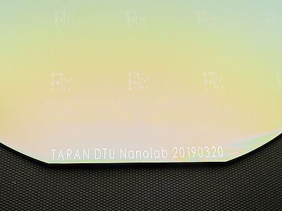
The conversion manager software allows for inclusion of labels during the design conversion process. The labels are configured in a .lbl tab-delimited ASCII file with a special header in the first row, which must be located in the 'HIMT\Designs\Labels' folder. When used, the labels defined in the label file will be merged with the pattern in the source file, and the result can be inspected in the viewer. The X and Y positions of the labels should be given in design coordinates, and will be subject to any offsets/shifts applied to the design. Note, that if the label file is changed, the job file will not update automatically.
Example of a label file:
X | Y | UNIT | HEIGHT | UNIT | TITLE
-16000 | -46000 | um | 2000 | um | TARAN DTU Nanolab 20190320
This produces a 2mm high, approximately 32mm long wafer ID at the flat of a 4" wafer. Some special characters are not allowed (e.g. ';').
Large defocus range
The standard range for the defocus parameter is -10 to 10, but a special feature allows to extend this range to -25 to 25. The large defocus range feature is set in the resist template, and can only be accessed by choosing the 'NLAB Large defoc range' resist template during the job setup. The dose must be set manually, as this is an otherwise empty resist template. Also, this feature will work in the entire range for pneumatic focus, but it will likely fail at the extremes for optical focus.
Technically, it is possible to combine this feature with other features, such as high aspect ratio mode, but this requires that at custom resist template is set up by staff.
High Aspect Ratio (DOF) mode
Aligner: Maskless 02 is configured with the so-called "Write Mode I", which uses a higher demagnification, higher NA lens system to achieve higher resolution. This reduces the depth of focus (technically depth of field), making it more difficult to achieve good lithographic results in thicker resist coatings. The theoretical DOF of Aligner: Maskless 02 is 0.3µm, compared to 1µm for Aligner: Maskless 01. In order to improve processing of thick resists, the Aligner: Maskless 02 has been configured with the High Aspect Ratio Mode, which uses a variable aperture in the optical path to decrease the (illumination) NA of the system, thus increasing the DOF at the expense of intensity and resolution limit.
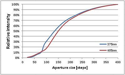
The aperture size is controlled via a parameter in the resist template. The high AR parameter can be Standard (aperture fully open; 800 motor steps), Large (100 steps), or X-Large (60 steps).
- Standard: No resist template or any normal resist template
- Large: 'NLAB High AR mode Large'
- X-Large: 'NLAB High AR mode XL'
Assuming a linear relation between motor steps and aperture diameter, Large corresponds to a relative aperture area of 1.6%, while X-Large corresponds to 0.6% aperture area. Intensity measurements show a relative intensity of approximately 25%, and 6%, respectively. The effective dose can be corrected by increasing the nominal dose in the exposure, either by a fixed machine parameter, or by the user setting a higher dose themselves. At the moment, the user will be required to increase the nominal dose.
Decreasing the aperture size significantly reduces the amount of light that reaches the sample, and thus the effective dose, as can be seen in the graph to the right, and the table below. The resolution limit, however, seem to be much less affected. Tests using 1.5µm MiR resist suggest that using the X-Large setting (60 steps) reduces the achievable resolution from 1µm at Standard setting to 3µm for exposure at 375nm, but only to 1.75µm for exposure at 405nm.
Dose factor for different wavelengths and aperture settings:
| 375nm | 405nm | |||
|---|---|---|---|---|
| Large (100) | X-Large (60) | Large (100) | X-Large (60) | |
| Intensity measurements | 3.3 | 17.4 | 5.7 | 14.6 |
| 150µm SU-8 acceptance test | ~3 | ~10 | NA | NA |
| 1.5µm AZ MiR 701 dose test | 7.5 | 20.8 | 6.7 | 18.0 |
| 10µm AZ 4562 dose test | ? | ? | ? | ? |
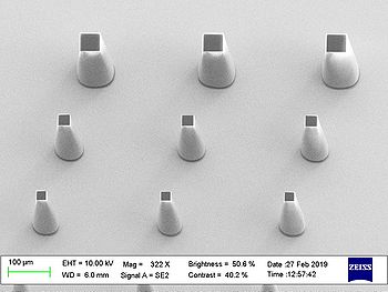
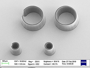
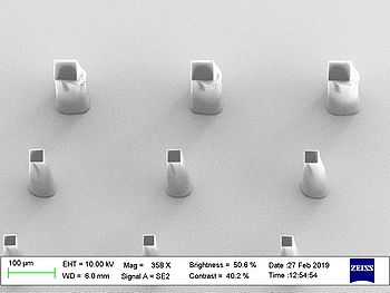
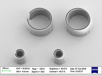
Results from acceptance test on 150µm thick SU-8:
| Pillars | Rings | |
|---|---|---|
| Standard (800)
6000 mJ/cm2 |
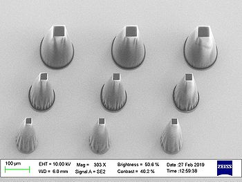
|
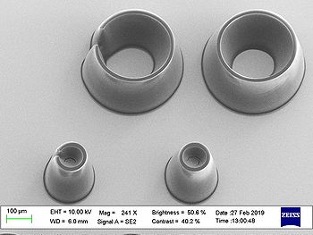
|
| Large (100)
16500 mJ/cm2 |
|
|
| X-Large (60)
55000 mJ/cm2 |
|
|
Alignment
This section is under construction 
The alignment accuracy of the Aligner: Maskless 02 is a combination of the position accuracy of the stage, the accuracy of the alignment mark detection, the accuracy of the pattern already on the wafer (first print), and the calibration of the machine (correction of offset between the exposure light axis and the center of the cameras). The calibration of the machine was performed during installation, but can also be corrected if systematic offsets are observed in alignment tests. This calibration also compensates errors in the detection of the alignment marks (at least on the standard samples used for calibration and alignment tests). By measuring the stitching accuracy between two layers printed on the same substrate (without unloading the substrate), we may be able to assess the stage accuracy. By aligning to a pattern previously exposed by the Aligner: Maskless 02, or ideally by another machine, we can assess the mask-less aligner's ability to compensate for any scaling and orthogonality errors between the two prints.
The results reported here use printed verniers to assess the misalignment along the two axes at different points on the wafer using an optical microscope. Two different designs were used; a ±5µm vernier and a ±1µm vernier. Both consist of a scale of 4µm lines with 10µm pitch, and a vernier scale to enable subdivision of the 5µm or 1µm scale into tenths, i.e. 0.5µm or 0.1µm. During inspection, observation of the symmetry of neighboring lines enables the observer to read the shifts with ±0.25µm or ±0.05µm accuracy.
The measurements are used to calculate the misalignment of the second layer with respect to the first print. The median of all measurement points in X or Y (reported as "Shift") is a measure for the average overall offset between the first and second print. At each point, this error is a combination of three contributions: The translational error ("Misplacement") is the amount by which the image is shifted; the run-in/run-out error ("Run-out") is the amount of gain in the image; and the rotational error ("Rotation") is the angle by which the image is rotated. The unit of ppm (parts per million) is used as rotation and run-out are generally small. A rotation of 1ppm corresponds to an angle of 0.2" (arcseconds) or a shift of 100nm across an entire 4" wafer, while a run-out of 1ppm corresponds to a shift of 50nm at the edge of a 4" wafer compared to the center. For comparison, the pixel size at the wafer surface is 160nm X 160nm, and the address grid size is 40nm. The deviations (±) given for the results here are calculated as half the range of measurements. If the range is smaller than the measurement uncertainty, the measurement uncertainty is used in stead. The samples used for these tests are 100mm Si wafers coated with a 1.5µm layer of positive tone resist (AZ 5214E or MiR 701).
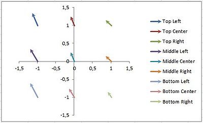
Stage stitching test:
| Shift (median) [µm] | Misplacement [µm] | Run-out (gain) [ppm] | Rotation [ppm] | ||
|---|---|---|---|---|---|
| 9 points, 60x60mm2 | X | -0.15±0.05 | -0.16±0.05 | 0.8±1.7 | -3.6±1.2 |
| Y | 0.25±0.125 | 0.26±0.11 | -0.3±1.7 | -0.3±1.2 | |
| All 25 points | X | -0.150±0.075 | |||
| Y | 0.250±0.125 | ||||
This test was performed by printing two layers on top of each other without unloading the substrate. There is no alignment performed, so it is a test of the stages ability to address the same spot twice. The first layer was a full 4" wafer, and was printed in ~½ hour. The second layer only consisted of alignment structures in a 5x5 grid, and printed in a few minutes.
The result shows significant misalignment between the two layers, higher than what is seen in true overlay tests. This is believed to be an effect of drift during the first, long print (most likely heating of the stage), as the misalignment is seen to be biggest between parts printed furthest apart in time (i.e. on the left side of the wafer). In a normal overlay print, this error can be at least partially compensated using the scaling and shearing function available for three or more alignment marks/positions.
Top Side Alignment
Overlay accuracy (spec): 0.5µm
Camera field of view (W x H):
High Res 64µm x 48µm
Low Res 213µm x 160µm
Overview 13mm x 10mm
Accessible stage coordinates:
High/Low Res X = ±108mm; Y = ±108mm
Overview X = ±108mm; Y = +39mm to -180mm
To be sure the Overview camera can be used to locate the first alignment mark, it is advised to use a mark in the bottom left portion (3rd quadrant) of the design as mark 1.
| MLA-MLA | Scaling [ppm] | Shearing [mRad] | Shift (median) [µm] | Misplacement [µm] | Run-out (gain) [ppm] | Rotation [ppm] | |
|---|---|---|---|---|---|---|---|
| 2 alignment marks
375nm, high res camera |
X | NA | NA | 0.25±0.15 | 0.25±0.05 | 1.7±1.7 | 2.2±1.3 |
| Y | NA | 0.3±0.13 | 0.29±0.05 | 0.8±1.7 | 0.0±1.7 | ||
| 4 alignment marks
375nm, high res camera |
X | -1 | 0.001 | 0.2±0.05 | 0.17±0.05 | -0.6±1.7 | 0.3±1.2 |
| Y | -1 | 0.4±0.05 | 0.42±0.05 | 0.6±1.7 | 0.6±1.2 | ||
| 4 alignment marks
375nm, low res camera |
X | -6 | 0.002 | -0.05±0.13 | -0.06±0.05 | -1.9±1.7 | 0.8±1.3 |
| Y | -2 | 0.3±0.05 | 0.3±0.05 | -0.6±1.7 | 1.1±1.7 | ||
Scaled first print:
| MLA-MLA | Scaling [ppm] | Shearing [mRad] | Shift (median) [µm] | Misplacement [µm] | Run-out (gain) [ppm] | Rotation [ppm] | |
|---|---|---|---|---|---|---|---|
| 4 alignment marks
375nm, high res camera |
X | 100 | 0.000 | -0.05±0.1 | -0.01±0.05 | 1.7±3.3 | 0.6±2.4 |
| Y | 101 | 0.2±0.05 | 0.18±0.05 | 0±3.3 | 0±2.4 | ||
| 4 alignment marks
375nm, high res camera |
X | not used | not used | -2.75±3.0 | -2.98±0.25 | -101±8.3 | -0.6±5.9 |
| Y | not used | 3.0±2.9 | 3.12±0.25 | -96.1±8.3 | 0.0±5.9 | ||
Back Side Alignment
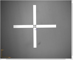
Overlay accuracy (spec): 1.0µm
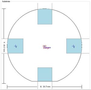
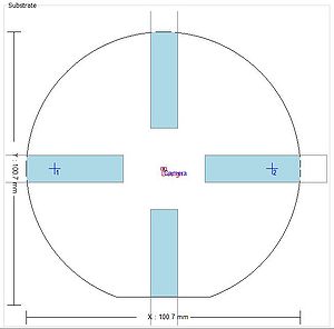
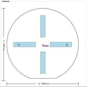
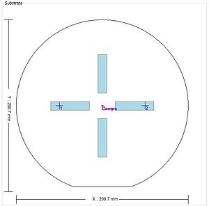
BSA windows: along the X and Y axes, 10mm x 46mm, starting 14.5mm from the center.
Camera field of view (W x H): 640µm x 480µm
|
|
|
|
| BSA marks positionned at x = ±20mm on a 2" wafer | BSA marks positionned at x = ±40mm on a 4" wafer | BSA marks positionned at x = ±50mm on a 6" wafer | BSA marks positionned at x = ±50mm on an 8" wafer |
| Offset (median) [µm] | Comment | ||
|---|---|---|---|
| Align-flip180-align, 3 points 375nm |
X | -0.625±0.125 | 0.5µm verniers, May 2019 |
| Y | -0.75±0.125 | ||
| Align-flip180-align, 3 points 405nm |
X | -0.625±0.125 | 0.5µm verniers, May 2019 |
| Y | -0.375±0.125 | ||
| KOH-window, ? points | X | 0.0±0.0 | Not performed yet |
| Y | 0.0±0.0 | ||
Advanced Field alignment (TSA)
Overlay accuracy (spec): 0.25µm (5x5mm2 area)
Shift, rotation, scaling, and shearing is determined and set by global alignment marks. The shift is corrected by automatic alignment to one mark in each field (chip).
| Shift (median) [nm] | Error (average) [nm] | ||
|---|---|---|---|
| 25 fields
375nm, high res camera |
X | 50±75 | 70±75 |
| Y | 150±50 | 128±50 | |
| Scaled first print, 10 fields
375nm, high res camera |
X | -25±50 | -5±50 |
| Y | 100±50 | 120±50 | |
| 25 fields
405nm, high res camera |
X | 100±75 | 108±75 |
| Y | 0±50 | 16±50 | |

