LabAdviser/Technology Research: Difference between revisions
No edit summary |
No edit summary |
||
| Line 4: | Line 4: | ||
The aim of this page is to give an overview of the technology research going on in the cleanroom and the other laboratories facilitated by DTU Nanolab. Here technology research projects will be presented. This includes a project description and links to other pages in LabAdviser where the process development outcome from these projects can be found. We urge all our users that do technology research at these facilities to present their activities here. At DTU Nanolab we commit our selves to present the technology research that we initiate to share the outcome with our users, as this is the main purpose for this research. | The aim of this page is to give an overview of the technology research going on in the cleanroom and the other laboratories facilitated by DTU Nanolab. Here technology research projects will be presented. This includes a project description and links to other pages in LabAdviser where the process development outcome from these projects can be found. We urge all our users that do technology research at these facilities to present their activities here. At DTU Nanolab we commit our selves to present the technology research that we initiate to share the outcome with our users, as this is the main purpose for this research. | ||
<!-- [[image:Technology Research.jpg|right|400px]] --> | <!-- [[image:Technology Research.jpg|right|400px]] --> | ||
'''Presentation Form for Presenting Technology Research:''' | |||
*[[/Presentation Form|Presentation Form]] | |||
If you perform technology research in the DTU Nanolab facilities, please contribute to this overview page. Start by contacting [mailto:labadviser@danchip.dtu.dk?Subject=I%20would%20like%20to%20present%20my%20technology%20research&body=Dear%20Berit,%0A%0DFree%20text...%0A%0DOr%20your%20call%20me:%2045256303 Berit Herstrøm]. | If you perform technology research in the DTU Nanolab facilities, please contribute to this overview page. Start by contacting [mailto:labadviser@danchip.dtu.dk?Subject=I%20would%20like%20to%20present%20my%20technology%20research&body=Dear%20Berit,%0A%0DFree%20text...%0A%0DOr%20your%20call%20me:%2045256303 Berit Herstrøm]. | ||
| Line 22: | Line 25: | ||
*[[/Organic Ice Resists for Electron-Beam Lithography - Instrumentation and Processes|Organic Ice Resists for Electron-Beam Lithography - Instrumentation and Processes]] - ''initiated November 2014'' | *[[/Organic Ice Resists for Electron-Beam Lithography - Instrumentation and Processes|Organic Ice Resists for Electron-Beam Lithography - Instrumentation and Processes]] - ''initiated November 2014'' | ||
*[[/Nanofabrication of Inductive Components for Integrated Power Supply On Chip|Nanofabrication of Inductive Components for Integrated Power Supply On Chip]] - ''initiated November 2014'' | *[[/Nanofabrication of Inductive Components for Integrated Power Supply On Chip|Nanofabrication of Inductive Components for Integrated Power Supply On Chip]] - ''initiated November 2014'' | ||
Revision as of 15:08, 13 March 2020
Feedback to this page: click here

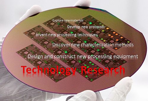
The aim of this page is to give an overview of the technology research going on in the cleanroom and the other laboratories facilitated by DTU Nanolab. Here technology research projects will be presented. This includes a project description and links to other pages in LabAdviser where the process development outcome from these projects can be found. We urge all our users that do technology research at these facilities to present their activities here. At DTU Nanolab we commit our selves to present the technology research that we initiate to share the outcome with our users, as this is the main purpose for this research.
Presentation Form for Presenting Technology Research:
If you perform technology research in the DTU Nanolab facilities, please contribute to this overview page. Start by contacting Berit Herstrøm.
Current Projects
- Smoothed advanced silicon NEMS devices - initiated November 2017
- Microfabrication of X-ray optical elements - initiated February 2017
Completed Projects
- Technology Development of 3D Silicon Plasma Etching process for Novel Devices and Applications - initiated November 2015
- Microfabrication of Hard x-ray Lenses - initiated December 2012
- Fabrication of Hyperbolic Metamaterials using Atomic Layer Deposition - initiated November 2013
- Nanoscale characterization of ultra-thin metal films for nanofabrication applications - initiated November 2014
- Organic Ice Resists for Electron-Beam Lithography - Instrumentation and Processes - initiated November 2014
- Nanofabrication of Inductive Components for Integrated Power Supply On Chip - initiated November 2014
