Specific Process Knowledge/Lithography/nLOF: Difference between revisions
Created page with "'''Feedback to this section''': '''[mailto:labadviser@danchip.dtu.dk?Subject=Feed%20back%20from%20page%20http://http://labadviser.danchip.dtu.dk/index.php/Specific_Process_Kno..." |
No edit summary |
||
| Line 2: | Line 2: | ||
AZ nLOF 2020 is a negative UV photoresist, suitable for loft-off processes. | AZ nLOF 2020 is a negative UV photoresist, suitable for loft-off processes. | ||
==Spin coating== | |||
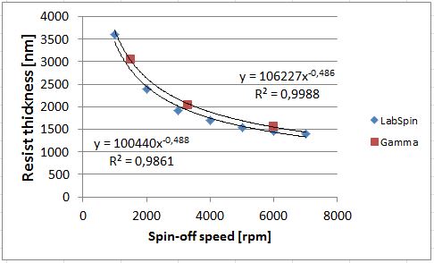
[[Image:nLOFspincurves.JPG|500x500px|thumb|Spin curves for AZ nLOF 2020 using a 30s spin-off, and a 60s@110°C softbake]] | |||
==Post-exposure bake== | ==Post-exposure bake== | ||
Revision as of 16:10, 23 July 2019
Feedback to this section: click here
AZ nLOF 2020 is a negative UV photoresist, suitable for loft-off processes.
Spin coating

Post-exposure bake
The recommended PEB for nLOF is 60s at 110°C, regardless of resist film thickness.
While 1min@110°C is adequate for Si substrates, less thermally conductive substrates (glass, III-V materials, chips bonded to carrier), have shoved problems using the standard PEB. These problems were largely solved by increasing the PEB time to 2min. Tests (on Aligner: Maskless 02) have shown that the lithographic performance of nLOF on Si is improved by using 2min@110°C PEB (less stitching, less bias, more negative profile).
Development
A 2µm nLOF resist film is fully developed in 20-30s using TMAH (AZ 726). However, the development can be continued to 60s in order to get a nore negative resist profile (increase the under-cut).
