Specific Process Knowledge/Etch/DRIE-Pegasus/Etch silicon nanostructures: Difference between revisions
No edit summary |
No edit summary |
||
| Line 22: | Line 22: | ||
| [[Image:DREM2pic1.jpg |frame|x300px|200nm trenches etched with 100 cycles (cross section view)]] | | [[Image:DREM2pic1.jpg |frame|x300px|200nm trenches etched with 100 cycles (cross section view)]] | ||
| [[Image:DREM2pic2.jpg |frame|x300px|200nm pillars etched with 100 cycles (cross section view)]] | | [[Image:DREM2pic2.jpg |frame|x300px|200nm pillars etched with 100 cycles (cross section view)]] | ||
|- | |||
| [[Image:DREM2pic3.jpg |frame|x300px|200nm pillars etched with 100 cycles (tilted view)]] | | [[Image:DREM2pic3.jpg |frame|x300px|200nm pillars etched with 100 cycles (tilted view)]] | ||
| [[Image:DREM2pic4.jpg |frame|x300px|Pillars etched with 100 cycles, patterns defined with EBL and ZEP resist, smallest dimesion of 100nm (tilted view)]] | | [[Image:DREM2pic4.jpg |frame|x300px|Pillars etched with 100 cycles, patterns defined with EBL and ZEP resist, smallest dimesion of 100nm (tilted view)]] | ||
|} | |} | ||
Revision as of 08:59, 26 April 2019
Feedback to this page: click here
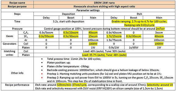
Based on the so called DREM process, there are two recipes on DRIE-Pegasus 1 which are suitable for etching silicon nanostructures. The recipes are called DREM 1kW nano and DREM 0.5kW nano. In DREM 1kW nano a higher coil power and larger gas flow rates are applied, making it suitable for etching high aspect ratio nanostructures (AR around 25 can be achieved depending on the patterns and resist used). In DREM 0.5kW nano both the coil power and gas flow rates are reduced, thus the scallop size can be reduced remarkably down to 16nm, giving a smooth sidewall on the nanostructures, while the aspect ratio can be limited. The recipes can be chosen based on the purpose of users, and the parameters are listed as below (different parameters are highlighted):
- Parameter settings DREM 1kW nano
-

- Parameter settings DREM 0.5kW nano
-


Below are some etched silicon nanostructures with the recipe DREM 1kW nano
 |
 |
 |
Below are some etched silicon nanostructures with the recipe DREM 0.5kW nano
 |
 |
 |
 |