|
|
| Line 22: |
Line 22: |
| * Nitrogen, also fully oxidized (oxidation state IV) | | * Nitrogen, also fully oxidized (oxidation state IV) |
| and plot their atomic percentages along with the percentages of oxygen and nitrogen. | | and plot their atomic percentages along with the percentages of oxygen and nitrogen. |
|
| |
|
| |
| == asdf ==
| |
|
| |
|
| |
|
| |
| {| border="1" cellpadding="0" cellspacing="0" style="text-align:center;"
| |
| | width="40" align="center" style="background:#f0f0f0;"|
| |
| | width="40" align="center" style="background:#f0f0f0;"|'''[[Specific_Process_Knowledge/Characterization/Optical_microscope| Optical Micro- scopes]]'''
| |
| | width="40" align="center" style="background:#f0f0f0;"|'''[[Specific Process Knowledge/Characterization/SEM: Scanning Electron Microscopy|SEM (incl. EDX)]]'''
| |
| | width="40" align="center" style="background:#f0f0f0;"|'''[[Specific Process Knowledge/Characterization/AFM: Atomic Force Microscopy|AFM]]'''
| |
| | width="40" align="center" style="background:#f0f0f0;"|'''[[Specific Process Knowledge/Characterization/Profiler|Stylus profiler]]'''
| |
| | width="40" align="center" style="background:#f0f0f0;"|'''[[Specific_Process_Knowledge/Characterization/Profiler#Optical_Profiler_.28Sensofar.29|Optical profiler]]'''
| |
| | width="40" align="center" style="background:#f0f0f0;"|'''[[Specific_Process_Knowledge/Characterization/Optical_characterization#Filmtek_4000|Filmtek (reflec- tometer)]]'''
| |
| | width="40" align="center" style="background:#f0f0f0;"|'''[[Specific_Process_Knowledge/Characterization/Optical_characterization#Ellipsometer|Ellip- someter]]'''
| |
| | width="40" align="center" style="background:#f0f0f0;"|'''[[Specific_Process_Knowledge/Characterization/Thickness_Measurer|Thickness stylus]]'''
| |
| | width="40" align="center" style="background:#f0f0f0;"|'''[[Specific_Process_Knowledge/Characterization/XPS#XPS-ThermoScientific|XPS]]'''
| |
| | width="40" align="center" style="background:#f0f0f0;"|'''[[Specific_Process_Knowledge/Characterization/PL_mapper|PL mapper]]'''
| |
| | width="40" align="center" style="background:#f0f0f0;"|'''[[Specific_Process_Knowledge/Characterization/4-Point_Probe|4-point probe]]'''
| |
| | width="40" align="center" style="background:#f0f0f0;"|'''[[Specific_Process_Knowledge/Characterization/Probe_station|Probe station]]'''
| |
| | width="40" align="center" style="background:#f0f0f0;"|'''[[Specific_Process_Knowledge/Characterization/XRD|XRD]]'''
| |
| | width="40" align="center" style="background:#f0f0f0;"|'''[[Specific_Process_Knowledge/Characterization/Lifetime_scanner_MDPmap|Life time scanner]]'''
| |
| | width="40" align="center" style="background:#f0f0f0;"|'''[[Specific_Process_Knowledge/Characterization/Drop_Shape_Analyzer|Drop shape analyser]]'''
| |
| | width="40" align="center" style="background:#f0f0f0;"|'''[[Specific_Process_Knowledge/Characterization/Hardness_measurement|Hardness tester]]'''
| |
| | width="40" align="center" style="background:#f0f0f0;"|'''[[Specific_Process_Knowledge/Characterization/DSC_Perkin_Elmer|Differen- tial Scan- ning Calori- meter DSC]]'''
| |
| | width="40" align="center" style="background:#f0f0f0;"|'''[[Specific_Process_Knowledge/Characterization/KLA-Tencor_Surfscan_6420|Surfscan]]'''
| |
| | width="40" align="center" style="background:#f0f0f0;"|'''IR-camera'''
| |
| | width="40" align="center" style="background:#f0f0f0;"|'''[[Specific Process Knowledge/Characterization/III-V_ECV-profiler|III-V ECV-profiler]]'''
| |
| |-
| |
| |-style="background:#C0C0C0;" align="center"
| |
| |align="left"| Breakdown voltage
| |
| ||||||||||||||||||||||||||||||||||||||||
| |
| |-
| |
| |-style="background:#DCDCDC;" align="center"
| |
| |align="left"| Carrier density/doping profile
| |
| ||||||||||||||||||||||||||||||||||||||||x
| |
|
| |
| |-
| |
| |-style="background:#DCDCDC;" align="center"
| |
| |align="left"| Charge carrier life time||||||||||||||||||||||||||||x||||||||||||
| |
| |-
| |
| |-style="background:#C0C0C0;" align="center"
| |
| |align="left"| Contact angle hydrophobic/hydrophillic||||||||||||||||||||||||||||||x||||||||||
| |
| |-
| |
| |-style="background:#DCDCDC;" align="center"
| |
| |align="left"| Crystallinity||||||||||||||||||||||||||x||||||||x||||||
| |
| |-
| |
| |-style="background:#C0C0C0;" align="center"
| |
| |align="left"| Deposition uniformity||||||||||x||x||x||||||||||||||||||||||||||
| |
| |-
| |
| |-style="background:#DCDCDC;" align="center"
| |
| |align="left"| Dimensions(in plane)||x||x||(x)||(x)||x||||||||||||||||||||||||||||||
| |
| |-
| |
| |-style="background:#C0C0C0;" align="center"
| |
| |align="left"|[[Specific_Process_Knowledge/Characterization/Topographic_measurement|Dimensions(height)]]||(x)||(x)||x||x||x||||||||||||||||||||||||||||||
| |
| |-
| |
| |-style="background:#DCDCDC;" align="center"
| |
| |align="left"| Electrical conductivity||||||||||||||||||||||||x||||||||||||||||
| |
| |-
| |
| |-style="background:#C0C0C0;" align="center"
| |
| |align="left"| [[Specific_Process_Knowledge/Characterization/Element_analysis|Element analysis]]||||x||||||||||||||x||x 4)||||||x 4)||||||||||||||
| |
| |-
| |
| |-style="background:#DCDCDC;" align="center"
| |
| |align="left"| [[Specific_Process_Knowledge/Characterization/Stress_measurement|Film stress]]||||||||x||||||||||||||||||x||||||||||||||
| |
| |-
| |
| |-style="background:#C0C0C0;" align="center"
| |
| |align="left"|[[Specific_Process_Knowledge/Characterization/Sample_imaging|Imaging]]||x||x||x||||x||||||||||||||||||||||||||||||
| |
| |-
| |
| |-style="background:#DCDCDC;" align="center"
| |
| |align="left"| [[Specific_Process_Knowledge/Characterization/Hardness_measurement|Material Hardness]]||||||||||||||||||||||||||||||||x||||||||
| |
| |-
| |
| |-style="background:#C0C0C0;" align="center"
| |
| |align="left"| Band gap||||||||||||||x||||||x||||||||||||||||||||
| |
| |-
| |
| |-style="background:#DCDCDC;" align="center"
| |
| |align="left"| Particles||x||x||x||||||||||||||||||||||||||||||x||||
| |
| |-
| |
| |-style="background:#C0C0C0;" align="center"
| |
| |align="left"| Phase changes||||||||||||||||||||||||||||||||||x||||||
| |
| |-
| |
| |-style="background:#DCDCDC;" align="center"
| |
| |align="left"| Reflectivity||||||||||||x||x||||||x 6)||||||||||||||||||||
| |
| |-
| |
| |-style="background:#C0C0C0;" align="center"
| |
| |align="left"| [[Specific_Process_Knowledge/Characterization/Measurement_of_film_thickness_and_optical_constants|Refractive index]]||||||||||||x||x||||||||||||||||||||||||||
| |
| |-
| |
| |-style="background:#DCDCDC;" align="center"
| |
| |align="left"| Resistivity||||||||||||||||||||||x||||||||||||||||||
| |
| |-
| |
| |-style="background:#C0C0C0;" align="center"
| |
| |align="left"| Step coverage||x 1)||x 1)||||||||||||||||||||||||||||||||||||
| |
| |-
| |
| |-style="background:#DCDCDC;" align="center"
| |
| |align="left"| Surface roughness||||||x||x||x||||||||||||||||||||||||||||||
| |
| |-
| |
| |-style="background:#C0C0C0;" align="center"
| |
| |align="left"| Thermal conductivity||||||||||||||||||||||||||||||||||||||||
| |
| |-
| |
| |-style="background:#DCDCDC;" align="center"
| |
| |align="left"| [[Specific_Process_Knowledge/Characterization/Measurement_of_film_thickness_and_optical_constants|Thin film thickness]]||x 1)||x 1)||x 2)||x 2)||x ||x||x||||||x 5)||x 3)||||x||||||||||||||
| |
| |-
| |
| |-style="background:#C0C0C0;" align="center"
| |
| |align="left"| Voids in wafer bonding||x||||||||||||||||||x||||||||||||||||||x||
| |
| |-
| |
| |-style="background:#DCDCDC;" align="center"
| |
| |align="left"| [[Specific_Process_Knowledge/Characterization/Thickness_Measurer|Wafer thickness]]||x 1)||x 1)||||||||||||x||||||||||||||||||||||||
| |
|
| |
| |-
| |
|
| |
|
| |
| |
| |
| |}
| |
Feedback to this page: click here
Depth profiling
The photoelectrons have a very short inelastic mean free path - this means that although generated at roughly equal numbers from the surface to deep inside the sample, only the photoelectrons emerging from the topmost layers will survive the passage to the surface unscattered. Photoelectrons that have undergone inelastic collisions will have lost a fraction of their kinetic energy - and hence no longer contribute to the intensity of the peak but will find itself in the rise in background signal on the left side of the peak in the spectrum (corresponding to lower kinetic energy).
This means that only atoms sitting in the topmost nanometers of the sample contribute to the intensity of the peak making the technique very surface sensitive. To access deeper layers of the sample one can use the argon ion gun to sputter off the surface layers of the sample - and then record a new set of spectra. A series with cycles of measurement with subsequent sputtering can be set up in this way creating a depth profile of the sample.
Example: Si wafer thin layers of oxide, nitride and polysilicon
Below is an example of a depth profile. The sample is a sandwich of:
- Silicon wafer
- Silicon oxide
- Silicon nitride
- Polysilicon
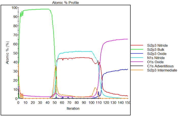
In the spectra required to make such a depth profile, one can distinguish the various chemical environments of silicon depending on whether it is bonded to:
- Silicon as in the bulk (oxidation state 0).
- Oxygen, either fully oxidized (oxidation state IV) in SiO2 or in intermediate states with a mixture of silicon and oxygen bonds (oxidation state I, II and III)
- Nitrogen, also fully oxidized (oxidation state IV)
and plot their atomic percentages along with the percentages of oxygen and nitrogen.
