Specific Process Knowledge/Characterization/SEM Supra 2: Difference between revisions
No edit summary |
|||
| Line 37: | Line 37: | ||
!colspan="2" border="none" style="background:silver; color:black;" align="center"|Equipment | !colspan="2" border="none" style="background:silver; color:black;" align="center"|Equipment | ||
|style="background:WhiteSmoke; color:black"|<b>SEM Supra 2 | |style="background:WhiteSmoke; color:black"|<b>SEM Supra 2 </b> | ||
|- | |- | ||
!style="background:silver; color:black" align="center" valign="center" rowspan="1"|Purpose | !style="background:silver; color:black" align="center" valign="center" rowspan="1"|Purpose | ||
Revision as of 13:23, 25 November 2019
Feedback to this page: click here

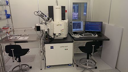
SEM Supra 2
The SEM Supra 2 is a scanning electron microscope. It produces enlarged images of a variety of specimens, achieving magnifications of over 500.000x providing ultra high resolution imaging. This important and widely used analytical tool provides exceptional resolution and depth of field and requires minimal specimen preparation.
The SEM is a VP (variable pressure) instrument - Indicating that it is capable of operating at variable pressure. By increasing the pressure in the chamber it is possible to image isolating samples. The higher density of gas molecules will eliminate the charges at the cost of slightly reduced resolution. Also, the Se2 and InLens detectors will no longer work.
This SEM has large chamber volume compared to the other SEMs at Danchip. An 8" wafer can be loaded in the chamber, however the X and Y ranges only provide full view of a 6" wafer.
All samples must be introduced into the chamber using an airlock. The airlock greatly reduces sample exchange times, and it accepts up to 8" wafer holders.
The SEM is equipped with an Oxford Instruments X-MaxN 50 EDX detector and AZtec software. EDX (Energy dispersive X-ray) detection is used for element composition analysis in a small area. A specific training is needed for users that want to use the EDX detector.
The SEM Supra2 in located in the cleanroom. It was installed in December 2013.
The user manual, control instruction, the user APV and contact information can be found in LabManager:
SEM Supra 2 info page in LabManager
Performance information
Equipment performances
| Equipment | SEM Supra 2 | |
|---|---|---|
| Purpose | Imaging and measurement of |
|
| Location |
| |
| Performance | Resolution |
The resolution is strongly dependent on the type of sample and the skills of the operator. |
| Instrument specifics | Detectors |
|
| Stage |
| |
| Electron source |
| |
| Operating pressures |
| |
| Options |
| |
| Substrates | Batch size |
|
| Allowed materials |
| |
