Specific Process Knowledge/Etch/KOH Etch: Difference between revisions
| Line 212: | Line 212: | ||
|} | |} | ||
<sup>{{fn|1}}</sup> Measured by Eric Jensen from DTU-Nanotech, October 2013. | <sup>{{fn|1}}</sup> Measured by Eric Jensen from DTU-Nanotech, October 2013. | ||
<br clear="all" /> | <br clear="all" /> | ||
Revision as of 16:56, 13 March 2018
Feedback to this page: click here
Si etch - Anisotropic silicon etch
KOH belongs to the family of anisotropic Si-etchants based on aqueous alkaline solutions. The anisotropy stems from the different etch rates in different crystal directions. The {111}-planes are almost inert whereas the etch rates of e.g. {100}- and {110}-planes are several orders of magnitude faster.
KOH-etching is a highly versatile and cheap way to realize micro mechanical structures if you can live with the necessary Si3N4- or SiO2-masking materials and the potassium contamination of the surface. The latter necessitates in most cases a wet post-clean ('7-up' or RCA-clean) if the wafer is to be processed further.
At Danchip we use as a standard a 28 wt% KOH. The etch rate - and the selectivity towards a SiO2-mask - is depending on the temperature. We normally use T=80 oC but may choose to reduce this to e.g. 60 oC or 70 oC in case of a high-precision timed etch (e.g. defining a thin membrane). In some cases we recommend to saturate the standard 28 wt% KOH with IPA with an etch temperature at T=70 oC (reduce evaporation of IPA). One example is for boron etch-stop, where the selectivity towards the boron-doped silicon is improved compared to the standard etch. Etching with IPA added to the KOH solution can be done in KOH fumehood.
- Different places to do anisotropic wet silicon etch
-
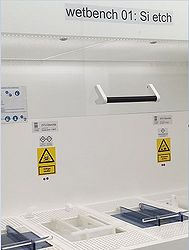 Wetbench 01: Si etch, for Si etch of 4" and 6" wafers using KOH. Positioned in cleanroom D-3.
 -
 Fume hood 06: Si etch, for Si etch of 4" and 6" wafers using KOH. Positioned in cleanroom D-3. This is used for wafers that are considered dirty.


The user manuals, quality control procedures and results, user APVs, technical information and contact information can be found in LabManager:
Si Etch 1: KOH info page in LabManager,
Si Etch 2: KOH info page in LabManager,
Si Etch 3: KOH info page in LabManager
Process Information
KOH etching baths
Key facts for the different etch baths available at Danchip are resumed in the table:
| Equipment | Si Etch 01 | Si Etch 02 | Si Etch 03 Fume hood 06 | |
|---|---|---|---|---|
| Purpose |
|
|
|
The bath is dedicated wafer with electroplated Nickel or otherwise dirty wafers |
| Link to safety APV and KBA | ||||
| Performance | Etch rates in crystalline silicon (100) |
|
|
|
| Etch rates in crystalline silicon (110) |
|
|
| |
| Etch rates in Thermal SiO2 |
|
|
| |
| Etch rates in other oxides |
. |
yannickseis@nbi.ku nov. 2017 @80 °C:
|
. | |
| Etch rates in SiN | ||||
| Roughness |
|
|
| |
| Anisotropy |
|
|
| |
| Process parameter range | Chemical solution |
KOH:H2O - 500 g : 1000 ml, when using pills KOH:H2O - 1000 ml: 1200 ml, when using premixed 50% KOH solution |
KOH:H2O - 500 g : 1000 ml, when using pills KOH:H2O - 1000 ml: 1200 ml, when using premixed 50% KOH solution |
|
| Temperature |
|
|
| |
| Substrates | Batch size |
|
|
|
| Size of substrate |
|
|
| |
| Allowed materials |
|
|
| |
| Masking material |
|
|
| |
1 Measured by Eric Jensen from DTU-Nanotech, October 2013.
Definition of <110> alignment structures
The etch rate dependence on the crystallographic planes can be used to determine the <110> crystal directions with high precision (better than +/- 0.05 o). A fast method for doing this, using the symmetric under-etching behavior around but not at the <110>-directions, was described by Vangbo and Bäcklund in J. Micromech. Microeng.6 (1996), 279-284. High-precision control of the <110>-direction during alignment can be necessary in order to control the dimensions of KOH-etched structures (e.g. precise control of V-groove dimensions). A dedicated mask (MASK NAME) has been designed for this purpose.
Etch rates: Empirical formula (Seidl et al)
The following empirical formula can be used for concentrations in the range of 10-60 wt%:
R = k0 [H2O]4 [KOH]0.25 e-Ea/kT,
where k0 = 2480 µm/hr (mol/l)-4.25, Ea = 0.595 eV for Si(100)
and k0 = 4500 µm/hr (mol/l)-4.25, Ea = 0.60 eV for Si(110)