Specific Process Knowledge/Etch/Etching of TOPAS: Difference between revisions
Appearance
No edit summary |
|||
| Line 1: | Line 1: | ||
<!--Checked for updates on 3/2-2016 - ok/jmli --> | <!--Checked for updates on 3/2-2016 - ok/jmli --> | ||
'''Feedback to this page''': '''[mailto:labadviser@nanolab.dtu.dk?Subject=Feed%20back%20from%20page%20http://labadviser.nanolab.dtu.dk/index.php/Specific_Process_Knowledge/Etch/Etching_of_TOPAS click here]''' | |||
==Etching of TOPAS== | ==Etching of TOPAS== | ||
Revision as of 12:47, 13 August 2019
Feedback to this page: click here
Etching of TOPAS
TOPAS is etched by an oxygen plasma in the ASE. Masking of TOPAS was achieved by photo resist or a hard mask of aluminum or silicon. Photo resist is the preferred masking material, since hard masks tends to introduce local masking due to redeposition. TOPAS can be etched at rates up to 500 nm/min, with excellent uniformity over the wafer.
| Parameter | Slow TOPAS etch | Fast TOPAS etch |
|---|---|---|
| O2 (sccm) | 50 | 99 |
| CO2 (sccm) (not available anymore) | 50 | 0 |
| Pressure (mTorr) | 40 | 40 |
| Coil power (W) | 800 | 720 |
| Platen power (W) | 60 | 60 |
| Temperature (oC) | 20 | 20 |
| Etch rate (nm/min) | ~350 | ~500 |
| Center-Edge uniformity | 0.98 | 0.95 |
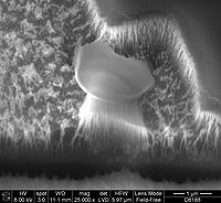
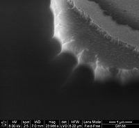
Under etching and local masking
When etching TOPAS I have in general used a hard mask material underneath my layer of photo resist, to ensure that if the resist was completely removed, a mask was still present. It is however always recomended to have a photo resist as mask, as a hard mask material will introduce roughness in unmask areas of the polymer.


