Specific Process Knowledge/Lithography/DUVStepperLithography: Difference between revisions
| Line 5: | Line 5: | ||
'''Feedback to this section''': '''[mailto:labadviser@danchip.dtu.dk?Subject=Feed%20back%20from%20page%20http://labadviser.danchip.dtu.dk/index.php?title=Specific_Process_Knowledge/Lithography/DUVStepperLithography#DUV_Stepper_FPA-3000EX4_from_Canon click here]''' | '''Feedback to this section''': '''[mailto:labadviser@danchip.dtu.dk?Subject=Feed%20back%20from%20page%20http://labadviser.danchip.dtu.dk/index.php?title=Specific_Process_Knowledge/Lithography/DUVStepperLithography#DUV_Stepper_FPA-3000EX4_from_Canon click here]''' | ||
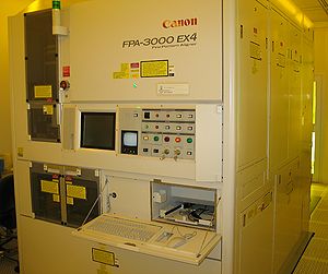
The deep-UV stepper FPA-3000EX4 from Canon is an advanced exposure system designed for mass-production of 6 and 8 inch wafers/ devices having a throughput of up to 90 wafers per hour. The largest applicable thickness of the wafers/ devices is 1,2 mm. Also 4" wafers/ devices can be processed with some restrictions concerning throughput, resolution, uniformity and maximum allowed wafer thickness. The system is equipped with a KrF Excimer laser from Cymer (wavelength 248 nm). Its projection lens’ NA is variable over a range between 0,4 and 0,6. Additionally, the partial coherence factor (sigma) of the illumination system can be adjusted and different off-axis illumination modes can be selected. | The deep-UV stepper FPA-3000EX4 from Canon is an advanced exposure system designed for mass-production of 6 and 8 inch wafers/ devices having a throughput of up to 90 wafers per hour. The largest applicable thickness of the wafers/ devices is 1,2 mm. Also 4" wafers/ devices can be processed with some restrictions concerning throughput, resolution, uniformity and maximum allowed wafer thickness. The system is equipped with a KrF Excimer laser from Cymer (wavelength 248 nm). Its projection lens’ NA is variable over a range between 0,4 and 0,6. Additionally, the partial coherence factor (&sigma) of the illumination system can be adjusted and different off-axis illumination modes can be selected. | ||
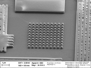
The critical dimension (CD) of patterns that can be realized is specified at around 250nm for arbitrary formed patterns in the standard illumination mode (NA=0,6; sigma=0,65). However, the best achievable resolution is different for each pattern type, pattern shape and pitch. So linewidths down to 160 nm could be achieved for geometrically simple patterns or pattern arrays (single and multiple line or pin-hole structures). | The critical dimension (CD) of patterns that can be realized is specified at around 250nm for arbitrary formed patterns in the standard illumination mode (NA=0,6; sigma=0,65). However, the best achievable resolution is different for each pattern type, pattern shape and pitch. So linewidths down to 160 nm could be achieved for geometrically simple patterns or pattern arrays (single and multiple line or pin-hole structures). | ||
Revision as of 13:34, 9 May 2016
DUV Stepper

Feedback to this section: click here
The deep-UV stepper FPA-3000EX4 from Canon is an advanced exposure system designed for mass-production of 6 and 8 inch wafers/ devices having a throughput of up to 90 wafers per hour. The largest applicable thickness of the wafers/ devices is 1,2 mm. Also 4" wafers/ devices can be processed with some restrictions concerning throughput, resolution, uniformity and maximum allowed wafer thickness. The system is equipped with a KrF Excimer laser from Cymer (wavelength 248 nm). Its projection lens’ NA is variable over a range between 0,4 and 0,6. Additionally, the partial coherence factor (&sigma) of the illumination system can be adjusted and different off-axis illumination modes can be selected.
The critical dimension (CD) of patterns that can be realized is specified at around 250nm for arbitrary formed patterns in the standard illumination mode (NA=0,6; sigma=0,65). However, the best achievable resolution is different for each pattern type, pattern shape and pitch. So linewidths down to 160 nm could be achieved for geometrically simple patterns or pattern arrays (single and multiple line or pin-hole structures).
The user manual(s), quality control procedure(s) and results and contact information can be found in LabManager:
Equipment info in LabManager
Process information
- Optimization and Simulation
- Reticle Design
- A DUV reticle is needed that should be designed by the customer. Please note that the projection magnification of the stepper is 1:5, so that the dimensions of the pattern on the reticle are expanded by a factor 5 with respect to those printed on the wafer.
The whole reticle can be regarded as one chip that might be printed one time onto the wafer or repeatedly - step-by-step - in a two dimensional array. Alternatively, different chips can be placed onto the reticle, separated by frames. These chips can be printed individually onto the wafer either as one chip or as an array. Then the individual chips of the design have to be surrounded by frames. Additionally, the pattern of two or more different reticles can be combined on one wafer.
If the pattern of the reticle must be aligned to another one - that is already located on the wafer - the wafer will need to be equipped with several alignment marks. A guide for preparing reticle files for the Canon FPA-3000EX4 stepper, having the correct dimensions and positions of the individual patterns, frames and alignment marks can be found here: File:Canon Stepper Reticle Guide v0 03.pdf.
Usually the reticle is fabricated by an external company. It is recommended to send the mask design in GDS format to the Photolith group of Danchip, so that they can verify the mask design and order the mask.
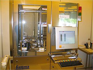
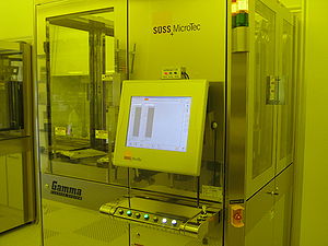
- The SÜSS Spinner-Stepper is dedicated for spinning DUV resists. Please note that a Bottom Anti-Reflective Coating (BARC) is necessary to guarantee high quality of both the resist film and the exposure. Please find the specification of the SÜSS Spinner-Stepper in the LabAdviser [Spinner-Stepper].
- Usually, in order to guarantee the highest fidelity of the produced pattern on the wafer the best suitable exposure dose has to be evaluated for each individual pattern, resist type and resist thickness. Thus, when a new reticle is used, it is recommended to perform an exposure dose test and - for resist thicknesses larger than 500 nm - additionally a focus offset test. After evaluation by SEM the identified dose and focus offset - that leads to the most accurate pattern - can be applied in the DUV process for the required wafers.
- The DUV process - including BARC and resist spinning, exposure, post exposure bake and development - will be performed by the customer together with the Photolith group of Danchip. Any kind of inspection, evaluation and pre- and post-processing should be performed by the customer.
| Purpose |
Exposure system designed for mass/production of devices with linewidth down to 250nm | ||
|---|---|---|---|
| Specifications | Magnification |
1:5 | |
| Projection lens Numerical Aperture |
0,4 - 0,60 | ||
| Illumination system's sigma |
0,2 - 0,75 (standard illumination mode: sigma = 0,65) | ||
| Exposure source |
KrF laser | ||
| Wavelength |
248nm | ||
| Illumination intensity |
2800 W/m2 | ||
| Illumination uniformity |
1,2% | ||
| Maximum printed field size |
22 x 26 mm (maximum on wafer) | ||
| Alignment accuracy |
3 sigma = 50 nm | ||
| Substrates | Substrate size |
| |
| Allowed materials |
| ||
| Batch |
1 - 25 | ||
SÜSS Spinner-Stepper

Feedback to this section: click here
This spinner is dedicated for spinning DUV resists. The spinner is fully automatic and can run up to 25 substrates in a batch 4", 6", and 8" size. The machine is equipped with the 3 resist lines, an automatic syringe system and a solvent line for cleaning and back-side rinse.
The user manual(s), quality control procedure(s) and results and contact information can be found in LabManager: Equipment info in LabManager
Process information
The spinning process will be performed by the customer together with the Photolith group of Danchip. In case you would like to do DUV lithography please contact Lithography team, who will consult you and run your wafers together with you.
Information about resist can be found here:
- Bottom Anti Reflection Coating (BARC) DUV 42S-6 .
- Datasheet DUV42S-6.
- Positive DUV resist for spinning in 300-600nm thickness range KRF M230Y.
- Positive DUV resist for spinning in 1600-800nm thickness range KRF M35G.
- Negative DUV resist for spinning in 1400-800nm or diluted with EC Solvent in 1:1 in 400-200nm thickness range UVN2300-0.8.
| Purpose |
| ||
|---|---|---|---|
| Resist |
| ||
| Performance | Coating thickness |
| |
| Process parameters | Spin speed |
10 - 5000 rpm | |
| Spin acceleration |
100 - 10000 rpm/s | ||
| Hotplate temperature |
| ||
| Substrates | Substrate size |
| |
| Allowed materials |
| ||
| Batch |
1 - 25 | ||
Developer TMAH Stepper

Feedback to this section: click here
This developer is dedicated for development of DUV resists. The developer is fully automatic and can run up to 25 substrates in a batch 4", 6", and 8" size. The machine is equipped with 1 developer line, in our case in 2,38% water based TMAH, 1 topside rinse line with water, 1 backside rinse line with water and 1 N2 line for drying.
The user manual(s), quality control procedure(s) and results and contact information can be found in LabManager: Equipment info in LabManager
Process information

The spinning process will be performed by the customer together with the Photolith group of Danchip. In case you would like to do DUV lithography please contact Lithography team, who will consult you and run your wafers together with you.
Here you can find a chart demonstrating a dependence between 250nm line width/pillors diameter and exposure dose.
| Purpose |
Development of DUV resist: KRF 230Y and KRF M35G | ||
|---|---|---|---|
| Developer |
2,38% water based TMAH | ||
| Process parameters | Spin speed |
10 - 5000 rpm | |
| Spin acceleration |
100 - 10000 rpm/s | ||
| Hotplate temperature |
130°C for post exposure baking | ||
| Substrates | Substrate size |
| |
| Allowed materials |
| ||
| Batch |
1 - 25 | ||
