Specific Process Knowledge/Characterization/SEM Supra 3: Difference between revisions
Appearance
No edit summary |
|||
| Line 22: | Line 22: | ||
!colspan="2" border="none" style="background:silver; color:black;" align="center"|Equipment | !colspan="2" border="none" style="background:silver; color:black;" align="center"|Equipment | ||
|style="background:WhiteSmoke; color:black"|<b>SEM Supra | |style="background:WhiteSmoke; color:black"|<b>SEM Supra 3 (Supra 40VP SEM)</b> | ||
|- | |- | ||
!style="background:silver; color:black" align="center" valign="center" rowspan="1"|Purpose | !style="background:silver; color:black" align="center" valign="center" rowspan="1"|Purpose | ||
| Line 45: | Line 45: | ||
*Secondary electron (Se2) | *Secondary electron (Se2) | ||
*Inlens secondary electron (Inlens) | *Inlens secondary electron (Inlens) | ||
* | *High Definition four quadrant Angular Selective Backscattered electron detector (HDAsB) | ||
*Variable pressure secondary electron (VPSE) | *Variable pressure secondary electron (VPSE) | ||
|- | |- | ||
|style="background:LightGrey; color:black"|Stage | |style="background:LightGrey; color:black"|Stage | ||
|style="background:WhiteSmoke; color:black"| | |style="background:WhiteSmoke; color:black"| | ||
*X, Y: | *X, Y: 130 × 130 mm | ||
*T: - | *T: -4 to 70<sup>o</sup> | ||
*R: 360<sup>o</sup> | *R: 360<sup>o</sup> | ||
*Z: 50 mm | *Z: 50 mm | ||
| Line 66: | Line 66: | ||
|style="background:LightGrey; color:black"|Options | |style="background:LightGrey; color:black"|Options | ||
|style="background:WhiteSmoke; color:black"| | |style="background:WhiteSmoke; color:black"| | ||
* | *High Definition four quadrant Angular Selective Backscattered electron detector (HDAsB) | ||
|- | |- | ||
!style="background:silver; color:black" align="center" valign="center" rowspan="3"|Substrates | !style="background:silver; color:black" align="center" valign="center" rowspan="3"|Substrates | ||
|style="background:LightGrey; color:black"|Batch size | |style="background:LightGrey; color:black"|Batch size | ||
|style="background:WhiteSmoke; color:black"| | |style="background:WhiteSmoke; color:black"| | ||
*Up to | *Up to 6" wafer with full view | ||
|- | |- | ||
| style="background:LightGrey; color:black"|Allowed materials | | style="background:LightGrey; color:black"|Allowed materials | ||
Revision as of 13:02, 2 May 2016
THIS PAGE IS UNDER CONSTRUCTION
Feedback to this page: click here

The user manuals, quality control procedures and results, user APVs, technical information and contact information can be found in LabManager:
SEM's at DTU Danchip:
- The SEM Leo page in LabManager,
- The SEM Supra 1 page in LabManager,
- The SEM Supra 2 page in LabManager,
- The SEM Supra 3 page in LabManager,
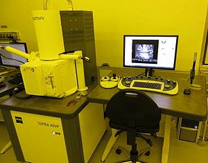
| Equipment | SEM Supra 3 (Supra 40VP SEM) | |
|---|---|---|
| Purpose | Imaging and measurement of |
|
| Location |
| |
| Performance | Resolution |
The resolution is strongly dependent on the type of sample and the skills of the operator. |
| Instrument specifics | Detectors |
|
| Stage |
| |
| Electron source |
| |
| Operating pressures |
| |
| Options |
| |
| Substrates | Batch size |
|
| Allowed materials |
| |
