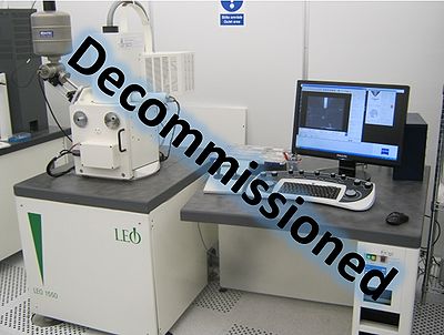
Specific Process Knowledge/Characterization/Lifetime scanner MDPmap: Difference between revisions
Appearance
| Line 39: | Line 39: | ||
* | * | ||
|- | |- | ||
!style="background:silver; color:black" align="center" valign="center" rowspan=" | !style="background:silver; color:black" align="center" valign="center" rowspan="2"|Instrument specifics | ||
|style="background:LightGrey; color:black"|Detector | |style="background:LightGrey; color:black"|Detector | ||
|style="background:WhiteSmoke; color:black"| | |style="background:WhiteSmoke; color:black"| | ||
| Line 51: | Line 51: | ||
*975 nm | *975 nm | ||
**Power 0.5 W to 4.0 W | **Power 0.5 W to 4.0 W | ||
*Spot diameter for all laser 0.5 µm | |||
|- | |- | ||
!style="background:silver; color:black" align="center" valign="center" rowspan="3"|Substrates | !style="background:silver; color:black" align="center" valign="center" rowspan="3"|Substrates | ||
|style="background:LightGrey; color:black"|Batch size | |style="background:LightGrey; color:black"|Batch size | ||
|style="background:WhiteSmoke; color:black"| | |style="background:WhiteSmoke; color:black"| | ||
* | *Sample sizs between 5 mm x 5 mm up to 16" or 210 mm x 210 mm | ||
*Sample thickness 10 µm to 20 mm | |||
* | |||
|- | |- | ||
| style="background:LightGrey; color:black"|Allowed materials | | style="background:LightGrey; color:black"|Allowed materials | ||
Revision as of 11:51, 16 November 2015
THIS PAGE IS UNDER CONSTRUCTION
Feedback to this page: click here

The user manual, control instruction, the user APV and contact information can be found in LabManager:
Lifetime scanner MPDmap info page in LabManager,
Performance information
| Equipment | ||
|---|---|---|
| Purpose |
| |
| Location |
| |
| Performance | Resolution |
|
| Instrument specifics | Detector | |
| Laser |
| |
| Substrates | Batch size |
|
| Allowed materials |
| |
