Specific Process Knowledge/Characterization/XPS/Processing/Basics/1intro: Difference between revisions
| Line 94: | Line 94: | ||
From this plot several points are open for discussion: | From this plot several points are open for discussion: | ||
* '''Which peaks to add''': The two spin-orbit doublets Si2p and Cu2p should be treated differently. The Si2p doublet peak is treated as one peak because of the small spin-orbit splitting (the splitting is 0.63 eV less than the 1 eV step size of the survey spectrum, see [[Specific Process Knowledge/Characterization/XPS/Processing/Basics/2highres#anchor_peaktable1|table in the next section]]). In contrast, the Cu2p doublet has some 20 eV's of spin-orbit splitting - as such the peaks may be fitted individually. The best way of fitting and quatinfying is to omit one of the peaks as is the case with the Zn2p doublet. This is easily done by removing the checkmark in the 'Q' column of one of the Cu2p peaks. | * '''Which peaks to add''': The two spin-orbit doublets Si2p and Cu2p should be treated differently. The Si2p doublet peak is treated as one peak because of the small spin-orbit splitting (the splitting is 0.63 eV less than the 1 eV step size of the survey spectrum, see [[Specific Process Knowledge/Characterization/XPS/Processing/Basics/2highres#anchor_peaktable1|table in the next section]]). In contrast, the Cu2p doublet has some 20 eV's of spin-orbit splitting - as such the peaks may be fitted individually. The best way of fitting and quatinfying is to omit one of the peaks as is the case with the Zn2p doublet. This is easily done by removing the checkmark in the 'Q' column of one of the Cu2p peaks. | ||
* '''Etching through thin layers: Probe depth and etch rates''': It looks as if the copper layer is contaminated with ZnO - at least the signals of Zn and O are not zero. | * '''Etching through thin layers: Probe depth and etch rates''': It looks as if the copper layer is contaminated with ZnO - at least the signals of Zn and O are not zero. There are several explanations for this: | ||
** The etching is too aggressive so the Cu layer is removed within too few levels. Lower the parameters of the ion bombardment to have more points. | |||
** The etching is non-uniform across the area that is probed. | |||
** The probing depth is long compared to the thickness of Cu layer. | |||
The data may be exported to Excel or Word by using the options on the 'W Reporting' tab next to the 'Display Modes' in the upper right corner of the GUI. | |||
Click [[Specific Process Knowledge/Characterization/XPS/Processing/Basics/2highres|here]] to continue the analysis. | Click [[Specific Process Knowledge/Characterization/XPS/Processing/Basics/2highres|here]] to continue the analysis on the high resolution spectra. | ||
<span id="anchor_1introbottom"></span> | <span id="anchor_1introbottom"></span> | ||
Revision as of 14:13, 11 September 2015
Open data and save the processing document
Locate the .VGX file in the experiment data tree. Either open the experiment by selecting 'Open Experiment' in Avantage, or double click on the .VGX file. You will see something like this:

It is a very good idea to save the processing document as you analyze the data (Avantage may crash some times) - to do so, select 'Save Processing Document' and you analysis will be saved as a .VGD file.
Spectrum views
To start analysing the data we will start by looking at the survey spectrum. Open a new processing document by clicking the button in the toolbar to the left as shown below:

This will spawn a tab with an empty processing grid.
Then drag the survey spectrum into one of the quadrants in the data grid as shown below:

Use the buttons as shown to the right below with the red square to
- Maximize spectrum views
- Minimize spectrum views
- Add or remove rows/columns

See section below on how to use the zoom capability.
Views of data with several levels
As shown (marked with a red square) in the bottom of the image below, some experiments hold several levels - the reason is that the exeriment is a depth profile in which a repeated set of spectra of a sample are recorded as the surface is gradually removed by an ion bombardment. Scroll through the individual levels, either by using the 'Etch time' or 'Etch Level' scroll buttons and see how the spectra change. Level 0 is the first spectrum.

The view called 'Single Trace' displays only one level - this button is highlighted in the top red square above. Change the display mode to view the complete set of levels by clicking the other buttons in the red square:
- Different views of spectra in experiments with several levels
-
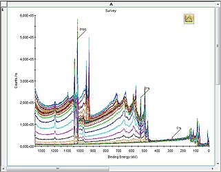 2D Chart view
 -
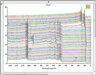 Stacked Chart view
 -
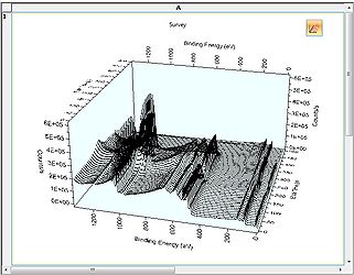 3D Chart view
 -
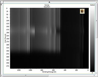 Image view


Zooming
There is two ways of zooming into the spectra:
- Press and hold SHIFT while dragging a square around the area of interest.
- Click the +magnifying glass and a drag a square.
Likewise, to cancel a zoom
- Press 'r' to reset the zoom.
- Click the Xmagnifying glass to cancel zoom.

Automatic peak identification of survey spectra
In the top are several buttons in the 'Analysis' toolbar. Click the leftmost one called Automatic Survey ID and a automated peak identification routine will commence. The result is shown below:

Several things are worth noting:
- A peak table pops up above the spectrum. It contains information (which elements, fitted atomic percentages etc.) obtained in the automatic fitting routine. One can still scroll through the levels (if more levels in a depth profile are available) but the elements fitted will not change.
- Only a fraction of the peaks in the spectrum have labels. The reason is that only the peaks from the peak table have a label - the remaining peaks in the spectrum are NOT unidentified elements but peaks (core levels or Auger transitions) of the elements already identified in the peak table.
Manually add peaks to identification of survey spectra
To add the peaks that are not present in current level (for copper and silicon), click 'Manual Peak ID' as shown below. A window called 'Manual Peak ID' opens - here select Cu and Si.

In the peak list below all peaks associated to the elements chosen will pop up. If you add all peaks in the table they will be part of the quantification. There is no reason to fit all peaks for each element, therefore make sure to restrict the quantification to the same peaks as the ones in the list of high resolution spectra - in this case select the Si2p and Cu2p peaks. Once the correct peaks have been chosen, press 'Add peaks' and 'Close'.
Make a depth profile from survey spectrum
With all peaks correctly identified and quantified, it is possible to make a depth profile from the data. First minimize the view to make the quadrants visible. Press 'Peak Table Profile' button as shown below and a window with different profile options will appear. Here, we select the 'Atomic %'.

This generates a plot in which the atomic percentage of each peak is plotted as a function of etch time.

From this plot several points are open for discussion:
- Which peaks to add: The two spin-orbit doublets Si2p and Cu2p should be treated differently. The Si2p doublet peak is treated as one peak because of the small spin-orbit splitting (the splitting is 0.63 eV less than the 1 eV step size of the survey spectrum, see table in the next section). In contrast, the Cu2p doublet has some 20 eV's of spin-orbit splitting - as such the peaks may be fitted individually. The best way of fitting and quatinfying is to omit one of the peaks as is the case with the Zn2p doublet. This is easily done by removing the checkmark in the 'Q' column of one of the Cu2p peaks.
- Etching through thin layers: Probe depth and etch rates: It looks as if the copper layer is contaminated with ZnO - at least the signals of Zn and O are not zero. There are several explanations for this:
- The etching is too aggressive so the Cu layer is removed within too few levels. Lower the parameters of the ion bombardment to have more points.
- The etching is non-uniform across the area that is probed.
- The probing depth is long compared to the thickness of Cu layer.
The data may be exported to Excel or Word by using the options on the 'W Reporting' tab next to the 'Display Modes' in the upper right corner of the GUI.
Click here to continue the analysis on the high resolution spectra.