Specific Process Knowledge/Lithography/EBeamLithography/JBX9500Manual: Difference between revisions
No edit summary |
|||
| Line 347: | Line 347: | ||
* In the SAVE window, click 'Acquisition of latest status' and (after the parameters appear in the window) click 'Apply/Save'. Note in the status line that the condition file has been saved. | * In the SAVE window, click 'Acquisition of latest status' and (after the parameters appear in the window) click 'Apply/Save'. Note in the status line that the condition file has been saved. | ||
= Exposure of mgn-files = | |||
<span style="font-size: 90%; text-align: right;">[[Specific_Process_Knowledge/Lithography/EBeamLithography/JBX9500Manual#top|Go to top of this page]]</span> | |||
#Open the exposure program, ‘Exp’, from the EBX Menu. | |||
#Find and load your magazine file: click ‘File/Magazine File’ and choose the magazine file from the location ‘/home/eb0/jeoleb/job/danchip’. | |||
#Check that the name of the desired magazine-file appears in the Magazine filename field, then click ‘Execute’. | |||
#Click ‘YES’ if you agree on the information in the ‘Pattern Writing Execution Check’-window. | |||
Before the exposure starts, some inital calibration will be performed such as CURRNT and HEIMAP. When measuring HEIMAP, the last saved condition of HEIMAP will be used. | |||
After finished exposure, the machine will display whether the exposure succeeded. | |||
= Alignment of wafers or chips = | |||
<span style="font-size: 90%; text-align: right;">[[Specific_Process_Knowledge/Lithography/EBeamLithography/JBX9500Manual#top|Go to top of this page]]</span> | |||
Alignment of wafer or chip requires specific training. | |||
First time you align on a type of wafer marks, you need to optimise the gain settings of the scan. The gain settings will depend on resist thickness, mark type (metal or etch) and substrate type. The gain settings can be found by the subprogram '''ACGRG'''. | |||
When the gain settings are known, you can execute '''SETWFR''' and '''CHIPAL'''. | |||
== AGCRG == | |||
<span style="font-size: 90%; text-align: right;">[[Specific_Process_Knowledge/Lithography/EBeamLithography/JBX9500Manual#top|Go to top of this page]]</span> | |||
{| cellpadding="2" style="border: 2px solid darkgray;" align="right" | |||
! width="500" | | |||
! width="500" | | |||
|- border="0" | |||
|[[File:AGCRG1.png|400px]] | |||
|[[File:AGCRG2.png|400px]] | |||
|- align="center" | |||
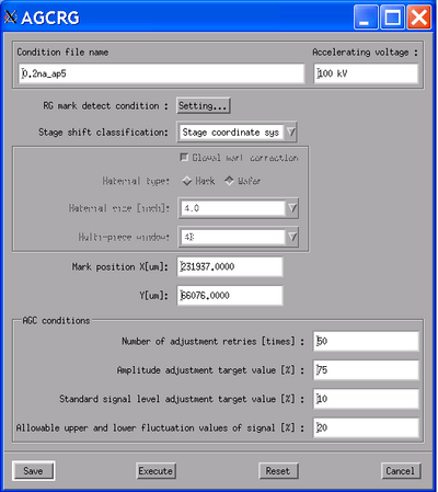
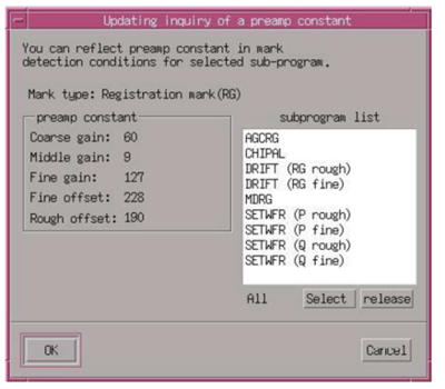
| Open and edit AGCRG, in the program window <br> '''1''' Enter the measured (from pre-aligner output) P mark position <br>'''2''' Click 'RG mark detect condition: Setting' and adjust scan width and position. Use a large scan width (200-600 microns). In 'Scan type' choose 'fine scan', 'box scan' and choose the correct mark (cross or L-shaped). Start with an 'X only' scan. <br>'''3''' Save and execute AGCRG || If the program finds the mark, ask the program to transfer the gain settings to SETWFR P (both rough and fine) or SETWFR Q. Scan again with same settings but choose 'Y only' in the 'RG mark detect conditions'. | |||
|} | |||
'''If the program does not find the mark''', try a larger scan width and execute AGCRG again, and/or try to scan 'Y only' instead. | |||
If the program still does not find the mark you can find it manually using the SEM. Remember to minimise the use of SEM: | |||
*Open the Stage program from EBX menu | |||
*In 'sspvideo' click beam/beam-off | |||
*'Move stage to mark position (setting/movement) | |||
*In 'sspvideo' click 'change/BE SEM' | |||
*open 'adjust' and 'Setting' and start the SEM. | |||
*Find the mark ROUGHLY and turn off the SEM again. | |||
Enter approximate mark position into AGCRG and execute AGCRG again. | |||
<br> | |||
<br> | |||
== SETWFR == | |||
<span style="font-size: 90%; text-align: right;">[[Specific_Process_Knowledge/Lithography/EBeamLithography/JBX9500Manual#top|Go to top of this page]]</span> | |||
[[File:SETWFR.png|600px]] | |||
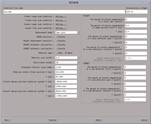
Before saving your condition file you should run the sub program 'SETWFR'. | |||
SETWFR will scan your P and Q marks and align the exposure to the position of these. | |||
From the calibration window, click 'SETWFR/Edit parameters'. Fill out the SETWFR parameters. | |||
*Choose measurement mode 'Semi Auto' | |||
*enter the material size and slot number (e.g 4A) | |||
*enter the material center offset (from the pre-alignment) and L-edit coordinates of P mark and Q mark. | |||
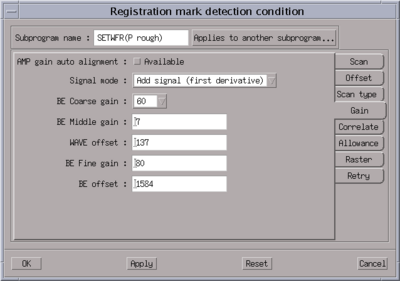
*In P-mark rough/fine scan settings, adjust scan settings and enter the width of your marks. Also check the gain settings are ok. | |||
*Repeat point 4 for Q-mark rough/fine | |||
*Click save and execute the program. | |||
Standard gain setting for gold wafer marks or etched marks (5-10 µm deep): | |||
<pre> | |||
BE Coarse gain 1 | |||
BE Middle gain 14 | |||
WAVE offset 128 | |||
BE Fine gain 128 | |||
BE offset 2020 | |||
</pre> | |||
'''When the subprogram 'SETWFR' has found the P and Q marks''' | |||
When SETWFR executes successfully feedback the 'P mark offset' to the OFFSET in the sdf file and re-compile the mgn-file. | |||
<br clear="all" /> | |||
[[File:RoughScan.png|400px|right]] | |||
[[File:RoughScanGain.png|400px|right]] | |||
'''If the program cannot find the marks''', you can either adjust the scan conditions, or gain settings. Also, test SETWFR again with 'OFFSET (P-mark)' from the pre-aligner output. | |||
Find the mark manually and let SETWFR scan the mark to align the sample: | |||
As a last alternative, you can chose to find the mark manually; this is however not recommended. | |||
SETWFR will ask you whether you wish to find the mark manually, click OK. | |||
*In 'sspvideo' click 'change/SEM' | |||
*open 'adjust' and 'Setting' and start the SEM. | |||
*Center the mark ROUGHLY and turn off the SEM again as fast as possible. | |||
* Click to continue the SETWFR scan at your present position | |||
*It might be necessary to repeat the procedure with the Q-mark. | |||
Please note that you should NOT align with the SEM but only roughly center the mark so you are sure the mark will be scanned with your scan settings. | |||
'''If SETWFR still cannot find your marks''' | |||
Unload the cassette, unmount your chip/wafer and remove the resist from your chip/wafer marks. Mount, pre-align and load your sample again and execute the exposure using manual alignment (see procedure in troubleshooting). | |||
<br clear="all" /> | |||
== CHIPAL == | |||
<span style="font-size: 90%; text-align: right;">[[Specific_Process_Knowledge/Lithography/EBeamLithography/JBX9500Manual#top|Go to top of this page]]</span> | |||
[[File:CHIPAL.png|500px]] | |||
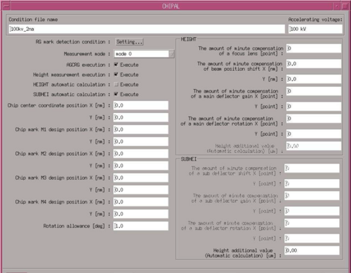
Before saving your condition file you should run the sub program 'CHIPAL'. | |||
CHIPAL will scan 1 or 4 of your chip marks and align the exposure to the position of these. Also, if HSWITCH is set to measure height in chip mark positions, the beam will be focused to the (average) height of the substrate near chip marks. | |||
During calibration, CHIPAL can be tested on one chip by the subprogram CHIPAL: | |||
From the calibration window, click 'CHIPAL/Edit parameters'. Fill out the CHIPAL parameters: | |||
*Choose 'mode 1' if you have 1 chip mark per chip or 'mode 4' if you have 4 chip marks per chip | |||
*If 'AGRCG' is executed, the machine will optimise the gain settings before mark detection; this is not recommended. Use instead same gain settings as in SETWFR. If the gain settings need to be adjusted for chip mark detection, use the subprogram 'AGRCG' on your chip mark (see section 7.1) | |||
*Leave 'Height measurement execution', 'HEIGHT' and 'SUBHEI' unmarked. | |||
*Enter the center position of one of your chips in 'Chip center coordinate position'; this position is in wafer coordinate systems. | |||
*Enter chip mark positions of M1-M4 in chip coordinate system, i.e. if you have a chip mark 1 mm x 1 mm from the center of the chip, M1 coordinates are (X,Y)=(1000,1000). | |||
*Save and execute the program. | |||
If the program can not detect your chip marks, change the scan conditions ('RG mark detection condition') and try again. | |||
<br clear="all" /> | |||
== Detailed descriptions of subprograms == | == Detailed descriptions of subprograms == | ||
| Line 701: | Line 848: | ||
<br> <br> | <br> <br> | ||
= Troubleshooting = | = Troubleshooting = | ||
Revision as of 21:27, 26 August 2015
Purpose, location and technical specifications
The JEOL JBX-9500FS electron beam lithography system is a spot electron beam lithography system designed for use in writing patterns (10 nm - 1 µm) in electron sensitive resists.
Substrates coated with resists are mounted in a cassette and transferred into the e-beam writer via the robot loader (autoloader). Even fully trained users are only authorized to mount substrates into the e-beam cassettes but not authorized to load the cassettes into the autoloader.
After your exposure, fully trained users can unload their cassettes from the autoloader, unmount their substrates and re-load an empty cassette into the autoloader.
If you are prohibited to unmount your substrates before another user requires the cassette, you must accept that either the next user or DTU Danchip personel unmount your substrates.
Location
The e-beam writer is located in a class 10 (ISO 4) cleanroom with tight temperature and moisture control. The room must only be entered when the machines or equipment inside the room is intended to be used. Always wear face-mask and an extra pair of gloves when handling cassettes.
The computer controlling the e-beam (EWS/9500) is located in the controller room which is a class 100 cleanroom area. The computers supporting the conversion of the e-beam files are also located in the controller room. Manuals
There are 3 manuals for the e-beam writer; apart from the main manual (this manual) there is a sdf and jdf-file manual, and a BEAMER manual. They can all 3 be accessed from LabAdviser or from LabManager under Technical documents.
The original JEOL manual for the e-beam writer JEOL JBX-9500FS is located on the O-drive: O:\CleanroomDrive\_Equipment\E-beam
Technical Specification.
Techical Specification
The system can be characterized as follows:
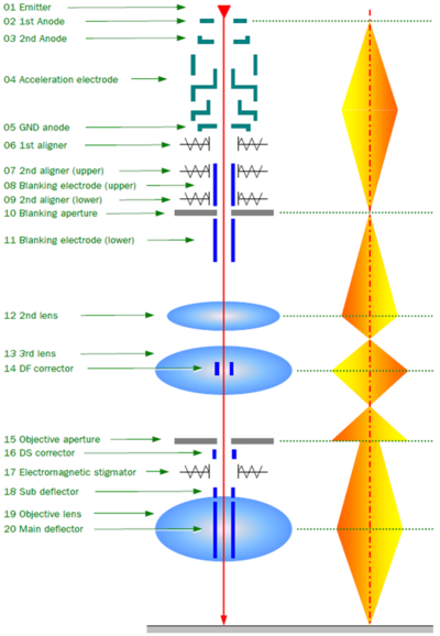
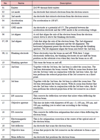
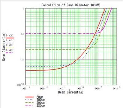
- The spot beam for electron beam writing is generated by a ZrO/W emitter and a four-stage electron beam focusing lens system, see illustration below.
- Electron-beam scanning speeds, f, up to 100 MHz are available (which is maximum scan speed).
- The acceleration voltage is 100 kV.
- The e-beam writer can pattern structures with a minimum resolution of 12 nm.
- The maximum field-size without stitching is 1000µm x 1000µm.
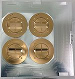
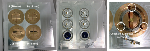
- The machine has cassettes that can contain either 6 wafers of 2” in size, 2 or 3 wafers of 4” in size, 1 wafer of 6” in size, 1 wafer of 8” in size, 4 chips of different sizes(slot sizes 4 mm, 8 mm, 12 mm, and 20 mm)
Rough estimation of exposure time
Pattern writing using the e-beam writer is implemented on a wafer or chip which has been coated with an electron sensitive resist. Both positive and negative types of resists for pattern writing can be used. In either case, the resist sensitivity Q (C/cm2) is a function of the beam current, I (A), the pattern writing area, A (cm2), and the pattern writing time t (s), as given below:
Q = It/A
The e-beam scanning frequency f (Hz) is a function of the e-beam scanning step, p (shot step), as shown below:
f = I /(Qp2)
The e-beam writer has scan speeds up to 100 MHz available. The dose, Q, shot step, p, and current, I, is chosen to meet the requirement of the pattern to be written, the writing time available, and also to meet the requirement f < 100MHz.
Based on the equations above, a rough estimate of the exposure time is easily calcualted. In the second sheet of the e-beam logbook, a simple program for calculating the scan speed frequency and an estimation of the exposure time can be found. Note, that the actual writing time will exceed this estimated exposure-time, as the exposure-time calculation does not include pre-calibrations and stage movement during exposure.
The area of your pattern can easily be found in L-edit by selecting all of your structure and use the area calculator in Tools/Add-Ins. If your pattern contains instances, you have to flatten your pattern (Cell/Flatten) before you use the area calculator; notice, however, that the flattening cannot be undone.
Mounting of chips or wafers into cassette
Authorized users are allowed to unload a cassette from the robot loader (autoloader) and mount their substrate but not allowed to load the cassette into the loader after mount.
We have one chip cassette, 2 2" cassettes, 2 4" cassettes, many 6" cassettes and 1 8" cassette. Some cassettes are made of Aluminum, others of Titanium. The thermal expansion coefficient of Ti is much lower than of Al; if the temperature difference of the cassette itself and the stage of the e-beam writer is lagre (> 0.1 degree), the expansion/compression during writing might be too large for critical patterns.
Keep an eye on the wafer orientation when you mount; the 2" aluminum cassette still have wafer orientation flat-up.
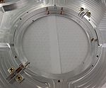
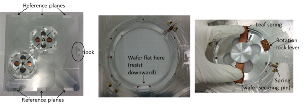
Wafer cassettes must be handled with great care and with an extra pair of clean gloves (to be found inside the e-beam room). Prevent any form of impact of the cassette and never touch the delicate parts of the cassette, i.e. the reference plane, reference marks or grounding pins. Take care that the cassette is not scratched against the metal table, always keep cleanroom side-sealed lintfree tissues between cassette and table.
General rules for handling cassettes and mounting wafers and chips into cassettes:
- Always wear face-mask and a new pair of gloves
- Never touch the reference planes, i.e. the six polished areas on the front side of the cassette
- Never lift the cassette in the hook
- Always check the wafer for loose parts or flakes before loading. In case of loose parts or flakes, stop mounting, discard or rework the sample and rethink your process.
- Always check the cassette for loose parts, dust and particles.
- For chips: Make sure the chip size is at least 2 mm larger than the slot opening. Be careful when mounting the plate; it will get stuck easily if mounted askew. Always check that the 12 large screws are tight.
- For wafers: When mounting a wafer, hold the spring (wafer securing pin) back when putting the wafer and the plate into the cassette, especially on the 2" cassette (the spring can lift the wafer). Tighten the leaf spring first, then release the spring and tighten the rotation lock lever.
- Inspect the front side of the cassette carefully after mounting the chip/wafer; a small gap between substrate and cassette will lead to a failure in HEIMAP and no exposure is thus possible.
Seen from the front-side of the cassette with the hook to the right, the workpiece windows (wafer positions) are named A, B, C etc in reading-direction from top left to bottom right.
Optical pre-alignment of wafers
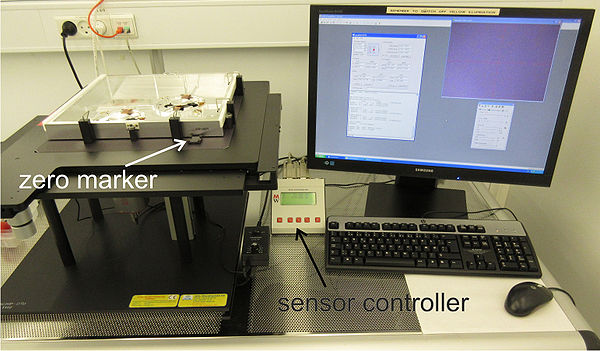
1. Carefully position the cassette face down on the optical aligner stage; make sure that the cassette is completely aligned with the stage before clamping the cassette to the stage. The hook of the cassette should turn away from yourself, i.e. towards the wall.
2. Open the Pre-Alignment Microscope System (PAMS) tool and Kappa Image Base from the Desktop. In Kappa Image Base, click ‘Open/Close Control Dialog’ in ‘Camera’. Click on the screen-icon to open camera view and the ‘>>’-icon to open the control dialog. If no contact can be reached to the camera via Kappa Image Base, restart the computer (login: cleanroom, password: Renrum12).
3. Turn on the yellow light. Align the stage to the zero-marker, and press x and y on the sensor controller. This zeros the position of the software according to zero of the stage. Always zero the stage at maximum magnification.
4. In PAMS, choose JBX-9300FS and correct wafer size and position in the workpiece window. Enter the P and Q mark design positions (i.e. L-edit coordinates).
5. Find the P mark at maximum magnification. Click ‘Get P’. Repeat the procedure with the Q mark. Calculate gain and rotation by clicking 'Calculate' and log the results in the Log-window by clicking 'Log result'. Switch off the yellow light after use.
6. Save the alignment information (File/Save). The file should be saved under your name and date, eg ‘mettekjan312012.txt’, in the folder ‘C:\temp’. This file can be transferred to the e-beam computer DCH1352 by email or dropbox.
7. In the jdf-file, the theoretical (L-edit/CleWin) position of the P and Q marks should be defined. In the sdf-file the mark-detection should be set to semi-automatic 'S' (see section 7 in this manual and the separate sdf- and jdf-file preparation manual).
Load and unload of cassettes into/from autoloader
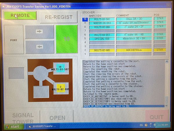
For safety reasons, users are only authorized to unload cassettes from the autoloader and to load empty cassettes into the autoloader.
Load and unload of cassettes into the autoloader can only be done via the touch-screen on the autoloader itself.
To load a cassette into the autoloader:
- Set the interface in LOCAL by clicking REMOTE (clicking this button toggles between REMOTE and LOCAL)
- Click OPEN and open the door
- Carefully put the cassette onto the platform with the hook away from yourself
- Close the door and click CLOSE
- Click the large green button (with number) until you reach the slot number you wish to load your cassette to
- Click arrow right. Confirm the transfer by clicking START (or click CANCEL if you regret). Do not change the comment.
- After transfer, set the autoloader back in REMOTE
To unload a cassette from the autoloader:
- Set the interface in LOCAL, by clicking REMOTE (clicking this button toggles between REMOTE and LOCAL)
- Click the large green button (with number) until you reach the slot number you wish to unload your cassette from
- Click arrow left. Confirm the transfer by clicking START (or click CANCEL if you regret).
- Click OPEN and open the door
- Carefully take the cassette from the platform and put it on the lint-free tissues on the table
- Close the door and click CLOSE
- Set the autoloader back in REMOTE
Transfer of cassettes between autoloader and e-beam writer
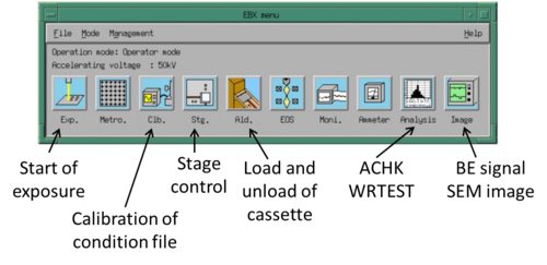
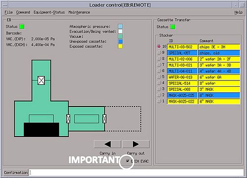
You can load the cassette into the e-beam writer from the loader control program (Ldr) from EBX Menu. This operation requires the autoloader to be in REMOTE.
To transfer a cassette from the autoloader into the e-beam writer:
- Choose the right cassette from the 'Stocker' window (red dot), and
- Click 'Carry in'
To transfer a cassette from the e-beam writer to the autoloader:
- Choose the right cassette from the 'Stocker' window (red dot)
- Tick the 'EXCH EVAC' on (This is important, otherwise you'll leave the exchange chamber ventilated)
- Click 'Carry out'.
If you by accident unload a cassette without evacuating the exchange-chamber, you must tick 'EXCH EVAC' and load your cassette onto stage and unload it to the autoloader again.
Calibration of condition file
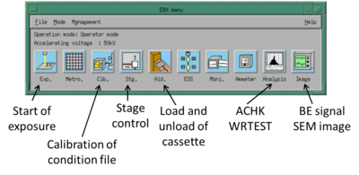
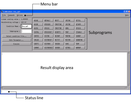
From the EBX menu on workspace 1, open the calibration window ‘Clb’. From this window, a previously used condition file (calibration file) dedicated to a certain aperture setting and current setting is loaded, re-calibrated, and saved again.
Calibration of condition files normally consists of a number of subprograms listed in the table below. The subprograms listed in the blue part of the table are a part of the 'daily' batch of programs.
| Calibration of condition files | |
|---|---|
| Subprogram | Explanation |
| CURRNT | The stage moves the Faraday's cup to the beam and the machine reads the value of the cup. The machine measures the beam current 5 times and calculate the average of the beam current based on these 5 measurements. |
| INITAE | The AE marks (Absorbed Electrons) is a mark type that is connected to a pn-junction, i.e. the current abosrbed in the mark is measured. The AE mark is a knife-edge mark, i.e. is has (originally) very sharp edges. When the beam (with a well-known frequency) scans over this type of mark and absorbed current simultanously is measured, an estimate of the beam diameter can be found. INITAE is a subprogram that finds the AE mark and scans it for testing that the machine can find the mark. |
| INITBE | The BE mark (Backscattered Electrons) is a mark type that consists of a suspended grid of metal. The openings in the grid is 500 microns in both X and Y. When the beam scans over this type of mark, backscattered electrons are detected with the BE detector inside the chamber. This type of mark is used to correlate stage position and beam position during calibration. INITBE is a subprogram that find the BE mark and scans it for testing that the machine can find the mark. |
| SFOCUS | This subprogram finds the minimum beam diameter by scanning an AE mark while changing the focus of the objective lens. The objective lens is defined to be in focus where the machine finds the minimum beam diameter. This program can also be used to observe the depth of focus of a certain condition file. The SFOCUS subprogram does not work well for currents above 6 nA, why SFOCUS is deleted in 'daily' routines of condition files with currents larger than 6 nA. |
| PDEFBE | Using a BE mark, this subprogram corrects deflection gain and rotation of the main deflector. The system positions the BE mark in the corners of the main field (which is a 1000 x 1000 µm2 square) and scans the mark using the primary deflector only. |
| DISTMEM | This subprogram measures the distortion of the beam deflection 7 x 7 positions within the main writing field and generates a distortion correction table. The system routinely positions the BE mark in all 49 positions and uses only the primary deflector to scan the BE mark in every 49 positions. The program sets the distortion directly below the beam (center of the field) to zero. The distortion correction memory in every position in the main writing field is generated by a linear approximation based on the 7 x 7 table. For 0.2 nA or 2 nA, a reasonable convergence value is e.g. 6 nm. |
| DISTBE | This subprogram measures the distortion of the beam deflection 7 x 7 positions within the main writing field and generates a distortion correction table. The system routinely positions the BE mark in all 49 positions and uses only the primary deflector to scan the BE mark in every 49 positions. The program sets the distortion directly below the beam (center of the field) to zero. The distortion correction memory in every position in the main writing field is generated by a cubic approximation based on the 7 x 7 table. For 0.2 nA or 2 nA, a reasonable convergence value is e.g. 8 nm. |
| SUBDEFBE | Using a BE mark, this subprogram corrects deflection gain and rotation of the secondary (sub) deflector. The system positions the BE mark in the corners of the subfield (which is a 4 x 4 µm2 square) and scans the mark using the sub deflector only. |
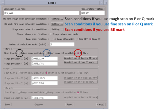
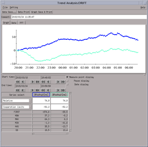
| DRIFT | This subprograms scans the DRIFT mark. The DRIFT mark can either be a BE mark or an alignment mark on the substrate. By scanning the DRIFT mark during exposure, the machine can positionally adjust the exposed pattern during writing, i.e. positional drift due to cassette heat-up or warm-up during writing can be corrected. This is done by using the the path DRF5M in the jdf-file. |
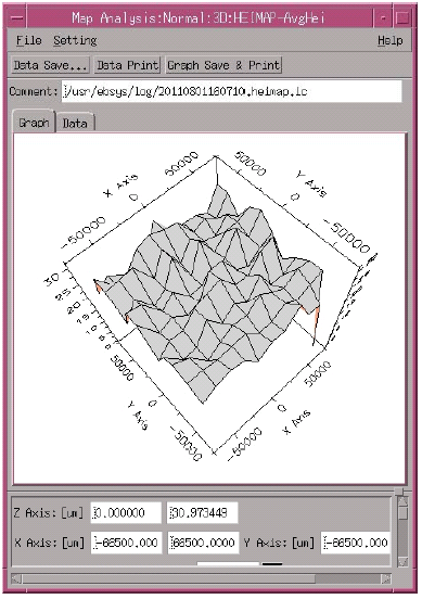
| HEIMAP | This subprogram measures the height of the substrate to be exposed. The size and workpiece position of the substrate (e.g. 4B) should be entered along with information of desired area to measure height. This area should always be larger than the area of the exposed pattern. The system will focus the beam to the average of the height mesaured in HEIMAP, but only if you expose in mask writing mode (i.e. no aligning) and execute HEIMAP in your initial calibration (e.g. by using path DRF5M). |
| SETWFR | This subprograms scans the global marks of the substrate. You need to enter the theoretical positions of the global marks (in wafer coordinate system) and the offset found during pre-aligning. When SETWFR has succeeded in finding your global marks, it will give you a corrected offset, that should be entered in your sdf-file. |
| CHIPAL | This subprogram scan a set of chip marks on the substrate. You need to enter theoretical position of a chip on your wafer (in wafer coordinate systems) and the theoretical positions of the chip marks on that chip (in chip coordinate system). CHIPAL will then scan 1 or 4 chip marks (mode 1 or mode 4). |
Calibration procedure
Load and restore a condition file
- Load and restore a condition file, click ‘Select condition file...’, choose the file from the list, e.g. ‘0.2nA_ap7’ and click OK. Restore the file by clicking ‘RESTOR/Edit Parameter...’. From the RESTOR window, click ‘Excecute’; the machine will now restore the conditions of the colum, this will take a few minutes. Exit the RESTOR window by clicking ‘Cancel’.
Execute CURRNT, INITAE, and INITBE
- Execute ‘CURRNT’ click ‘CURRNT/Execute’. The program ends by stating the average value of five measurements of the e-beam current; write this average current in the logbook.
- Execute INITAE; click 'INITAE/Execute'.
- Execute INITBE; click 'INITBE/Execute'.
If the machine cannot find the marks: Increase scan width to 40 µm and execute the subprogram again. Inspect the troubleshooting section for detailed instructions.
Execute 'daily'
- Execute the pre-defined set of sub-programs called ‘daily’: click 'Commands/Batch...'. Click ‘Condition file...’, choose ‘daily’, and click OK and execute. This set of programs takes around 8-10 minutes to run.
Execute DRIFT
- Click 'DRIFT' and 'Edit parameters'.
- Select ‘Acquisition of bottom BE mark’, and click ‘Save’ and ‘Execute’. Exit the window by clicking ‘Cancel’.
- If you are calibrating the high current of a double-current exposure you should increase the scan width to 40 microns and note the position of the drift mark. When calibrating the low current of a double-current exposure, make sure DRIFT scans the same drift mark as the high-current condition file.
- Read the subsection on DRIFT subprogram if you wish to use a global mark as DRIFT mark (recommended in certain cases)
Execute HEIMAP
- Click 'HEIMAP' and 'Edit parameters'.
- In the HEIMAP window, you should type in the correct substrate type and workpiece window.
- Measure 5 x 5 points in X and Y
- Adjust the pitch (µm) of the 5 points in X and Y to cover the entire pattern on your substrate.
- Click ecxecute. Repeat HEIMAP for all substrates on stage (e.g. 4A and 4B)
- click 'Cancel' when HEIMAP have been executed on all substrates
Execute SETWFR and CHIPAL
If you have alignment of your pattern to an existing pattern on your substrate. Read more about SETWFR and CHIPAL in the subsections below.
Execute SAVE
- Click 'SAVE' and 'Edit parameters'
- In the SAVE window, click 'Acquisition of latest status' and (after the parameters appear in the window) click 'Apply/Save'. Note in the status line that the condition file has been saved.
Exposure of mgn-files
- Open the exposure program, ‘Exp’, from the EBX Menu.
- Find and load your magazine file: click ‘File/Magazine File’ and choose the magazine file from the location ‘/home/eb0/jeoleb/job/danchip’.
- Check that the name of the desired magazine-file appears in the Magazine filename field, then click ‘Execute’.
- Click ‘YES’ if you agree on the information in the ‘Pattern Writing Execution Check’-window.
Before the exposure starts, some inital calibration will be performed such as CURRNT and HEIMAP. When measuring HEIMAP, the last saved condition of HEIMAP will be used.
After finished exposure, the machine will display whether the exposure succeeded.
Alignment of wafers or chips
Alignment of wafer or chip requires specific training.
First time you align on a type of wafer marks, you need to optimise the gain settings of the scan. The gain settings will depend on resist thickness, mark type (metal or etch) and substrate type. The gain settings can be found by the subprogram ACGRG.
When the gain settings are known, you can execute SETWFR and CHIPAL.
AGCRG
If the program does not find the mark, try a larger scan width and execute AGCRG again, and/or try to scan 'Y only' instead.
If the program still does not find the mark you can find it manually using the SEM. Remember to minimise the use of SEM:
- Open the Stage program from EBX menu
- In 'sspvideo' click beam/beam-off
- 'Move stage to mark position (setting/movement)
- In 'sspvideo' click 'change/BE SEM'
- open 'adjust' and 'Setting' and start the SEM.
- Find the mark ROUGHLY and turn off the SEM again.
Enter approximate mark position into AGCRG and execute AGCRG again.
SETWFR
Before saving your condition file you should run the sub program 'SETWFR'.
SETWFR will scan your P and Q marks and align the exposure to the position of these.
From the calibration window, click 'SETWFR/Edit parameters'. Fill out the SETWFR parameters.
- Choose measurement mode 'Semi Auto'
- enter the material size and slot number (e.g 4A)
- enter the material center offset (from the pre-alignment) and L-edit coordinates of P mark and Q mark.
- In P-mark rough/fine scan settings, adjust scan settings and enter the width of your marks. Also check the gain settings are ok.
- Repeat point 4 for Q-mark rough/fine
- Click save and execute the program.
Standard gain setting for gold wafer marks or etched marks (5-10 µm deep):
 BE Coarse gain  1
 BE Middle gain 14
 WAVE offset    128
 BE Fine gain   128
 BE offset      2020
When the subprogram 'SETWFR' has found the P and Q marks
When SETWFR executes successfully feedback the 'P mark offset' to the OFFSET in the sdf file and re-compile the mgn-file.
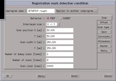
If the program cannot find the marks, you can either adjust the scan conditions, or gain settings. Also, test SETWFR again with 'OFFSET (P-mark)' from the pre-aligner output.
Find the mark manually and let SETWFR scan the mark to align the sample:
As a last alternative, you can chose to find the mark manually; this is however not recommended.
SETWFR will ask you whether you wish to find the mark manually, click OK.
- In 'sspvideo' click 'change/SEM'
- open 'adjust' and 'Setting' and start the SEM.
- Center the mark ROUGHLY and turn off the SEM again as fast as possible.
- Click to continue the SETWFR scan at your present position
- It might be necessary to repeat the procedure with the Q-mark.
Please note that you should NOT align with the SEM but only roughly center the mark so you are sure the mark will be scanned with your scan settings.
If SETWFR still cannot find your marks
Unload the cassette, unmount your chip/wafer and remove the resist from your chip/wafer marks. Mount, pre-align and load your sample again and execute the exposure using manual alignment (see procedure in troubleshooting).
CHIPAL
Before saving your condition file you should run the sub program 'CHIPAL'.
CHIPAL will scan 1 or 4 of your chip marks and align the exposure to the position of these. Also, if HSWITCH is set to measure height in chip mark positions, the beam will be focused to the (average) height of the substrate near chip marks.
During calibration, CHIPAL can be tested on one chip by the subprogram CHIPAL: From the calibration window, click 'CHIPAL/Edit parameters'. Fill out the CHIPAL parameters:
- Choose 'mode 1' if you have 1 chip mark per chip or 'mode 4' if you have 4 chip marks per chip
- If 'AGRCG' is executed, the machine will optimise the gain settings before mark detection; this is not recommended. Use instead same gain settings as in SETWFR. If the gain settings need to be adjusted for chip mark detection, use the subprogram 'AGRCG' on your chip mark (see section 7.1)
- Leave 'Height measurement execution', 'HEIGHT' and 'SUBHEI' unmarked.
- Enter the center position of one of your chips in 'Chip center coordinate position'; this position is in wafer coordinate systems.
- Enter chip mark positions of M1-M4 in chip coordinate system, i.e. if you have a chip mark 1 mm x 1 mm from the center of the chip, M1 coordinates are (X,Y)=(1000,1000).
- Save and execute the program.
If the program can not detect your chip marks, change the scan conditions ('RG mark detection condition') and try again.
Detailed descriptions of subprograms
SFOCUS
PDEFBE
By using the (bottom) BE mark (specified in INITBE), the machine measures the gain and rotation of the main deflector (Primary DEFlector using BE mark).
The machines measures over a field specified in the subprogram but no larger than the main field size (1 mm x 1 mm).
The output of PDEFBE looks like this:
| ========= PDEFBE Final result (0.2nA ap5) ================== |
|---|
Field size [um] = 960.0000 Number of bottom mark retries = 1 Deflector = PDEF Previous DAC[point] Shift value[nm] Corrected DAC[point] GAIN (X Y) = -9320 -9932 0.0 1.4 -9323 -9936 ROT (X Y) = 17541 17800 -0.5 -0.6 17543 17806 Height conversion conefficient = 0.435090 Height offset = -138.560000 Height correction coefficient X Y GAIN X,Y = 1.121066e+01 1.123170e+01 ROT X,Y = -4.416959e+00 -4.248694e+00 Distortion conversion coefficient X Y GAIN X,Y = 0.000000e+00 0.000000e+00 ROT X,Y = 0.000000e+00 0.000000e+00 Reference height [um] = 0.667 difference between the bottom BE mark and the reference plane [um] = -0.064 difference between the top BE mark and the bottom BE mark [um] = 47.544 =========================================================================================== |
The most important output of PDEFBE is the gain shift value which is 1.4 nm (in Y); the maximum allowable gain correction in this condition file (0.2nA ap5) is 6 nm. If PDEFBE did not reach a shift value below 6 nm within 3 retries for this condition file, the scan position on the BE mark should be shifted or a new BE mark should be used instead.
DISTMEM and DISTBE
DISTMEM and DISTBE measures the distortion of the beam over the entire writing field, i.e. positional errors in the beam over the entire writing field. Both programs use the bottom BE mark to detect these errors. The stage moves the mark to 7 x 7 positions distributed over 1 x 1 mm^2 writing field. At each position, the beam is deflected by the primary deflector to scan the mark. The distortion is defined as the offset between the actual stage position and position of the mark measured by the beam.
After measuring all 7 x 7 points, the machine generate a distortion correction table and measures again. This procedure is repeated until the maximum offset is as specified in 'allowable convergence value' in DISTBE or DISTMEM.
DISTBE generates the correction table for every position in the main writing field by cubic approximation between measurement points. DISTMEM generates the correction table for every position in the main writing field by linear approximation between measurement points.
We empirically found that executing DISTMEM before executing DISTBE gives the best results.
If the convergence value is not met after 3-4 measurements, the scan position on the BE mark should be changed as described in troubleshooting.
| ========= OUTPUT of DISTBE Final result (2nA ap5) ================== |
|---|
[Measurement information]
	Linear scaling value      = 1.000000
	Start time                = Wed May  6 12:02:27 2015
	End time                  = Wed May  6 12:08:50 2015
	Measurement result file   = 20150506120227.distbe.bat.ic

	Deflector                 = PDEF

[Height measurement]
	Reference height              [um] =       0.000

[Main deflector result]
DISTBE measurement condition information
	Register clear mode                = Off
	Field size                    [um] =    980.0000
	Zigzag                             = X -> Y
	Measurement starting point         = Top left
	Number of to-and-fro measurements  =           1
	Number of measurement points in the 1st quadrant =           4
	Measurement pitch [ 1/ 3]     [um] =    163.3000
	Measurement pitch [ 2/ 3]     [um] =    163.3000
	Measurement pitch [ 3/ 3]     [um] =    163.4000
	Stage fixing flag                  = Stage shift
	Number of retries                  =           1


Amount of field center shift                     X, Y [nm] =        -2.2          0.7
Scanning position                                X, Y [nm] =    -17200.0     -17200.0

distortion result [nm]
     X      |  -490.0000 |  -326.7000 |  -163.4000 |     0.0000 |   163.4000 |   326.7000 |   490.0000 |
------------+-------------------------------------------------------------------------------------------
   490.0000 |        3.3         -2.1         -1.7         -1.4         -2.9         -2.9          2.7
   326.7000 |       -4.0         -1.3         -1.3         -1.2         -1.1         -2.2         -1.8
   163.4000 |       -3.0         -1.1         -0.6         -0.2         -0.6         -1.2         -1.7
     0.0000 |       -1.6         -0.3          0.1          0.0         -0.3         -0.4         -1.9
  -163.4000 |       -1.0         -0.7          0.0         -0.5          0.0         -0.5         -1.1
  -326.7000 |       -3.2         -1.6         -0.9         -0.7         -0.8         -1.6         -2.9
  -490.0000 |        3.3          3.1         -2.9         -3.0         -3.1          1.4          1.4


     Y      |  -490.0000 |  -326.7000 |  -163.4000 |     0.0000 |   163.4000 |   326.7000 |   490.0000 |
------------+-------------------------------------------------------------------------------------------
   490.0000 |        1.3         -5.5         -1.9         -2.9         -3.8          3.9          2.9
   326.7000 |       -2.0         -1.2          1.7         -1.0         -3.1          2.6         -2.6
   163.4000 |       -1.7         -1.2          0.1         -2.7         -4.4          2.4         -2.4
     0.0000 |       -2.4         -0.4          3.2          0.0         -2.9          3.9         -1.9
  -163.4000 |       -2.1          0.4          3.1         -0.7         -4.8          0.3         -5.0
  -326.7000 |       -0.9          0.1          1.8         -0.9         -3.0          3.7         -3.6
  -490.0000 |        2.6          2.4          1.5         -2.0         -5.2          1.9          1.2
|
SUBDEFBE
By using the (bottom) BE mark (specified in INITBE), the machine measures the gain and rotation of the subsidary (secondary) deflector (SUBsidary DEFlector using BE mark).
The machines measures over a field specified in the subprogram but no larger than the main field size (4 µm x 4 µm).
DRIFT
You can choose any mark as a DRIFT mark. In a standard exposure, a (bottom plane) BE mark is used as DRIFT mark, but you can ask the machine to use one of your global marks as well, i.e. P or Q marks. This requires alignment in semi-automatic mode, however.
HEIMAP
Mask writing mode (first print)
With the path DRF5M, which is recommended for first print exposures (mask writing mode), HEIMAP is executed right before the machine starts the exposure and the machine will use the HEIMAP settings saved at this point.
The e-beam software can only save and use one pitch-setting, even if you expose two wafers/chips. Therefore, perform and save HEIMAP with the settings you wish to perform right before exposure.
Direct writing mode (with alignment)
When the exposure is performed in direct writing mode, i.e. the pattern is aligned to P and Q marks on the wafer and/or virtual chip mark detection is obtained, the result of HEIMAP is discarded and can be omitted in initial calibration. In this case, HEIMAP can be executed to check the substrate has been mounted correctly in the cassette.
It is important to measure height over an area that cover the entire pattern to be exposed. Also, make sure not measure height too close to the rim of the cassette (0.5-1 cm depending on cassette) or at substrate positions where the laser beam is deflected from holes or mesas.
SETWFR
SETWFR is the subprogram that finds and scan your global marks, i.e. P and Q marks.
Before executing SETWFR you should edit the parameters. Enter
- Measurement mode: Choose Semi-automatic.
- Material type: Wafer
- Material size: your substrate size, choose 3.0 if you expose on a chip
- Multi-piece window: the position of your substrate
- Allowable rotation value: 2-10 degrees
- Material Center offset position: Enter the offset found in your pre-align measurement
- P (and Q) point design position (material system): enter the position of your P (and Q) mark in wafer/chip coordinate system.
Save the subprogram and execute it.
If it does not work, the machine will ask you whether you wish to find the marks manually by using the SEM. Before you do that, adjust the parameters of SETWFR with one (or all) of the follwing things and execute SETWFR again:
- Increase the rough scan width of both P and Q mark to around 300 µm
- Set the BE coarse gain to 60 in the rough scan of P and Q mark (see under 'Gain' tab)
- Change the interlaced scan from 'X -> Y' to 'Y -> X', 'X only', or 'Y only' (see under 'Scan' tab)
If nothing of the above work, accept to find the mark manually by using the SEM. Please be aware that you should only roughly find the mark with the SEM, i.e. center it on the screen, and not align with the SEM.
When SETWFR has been executed succesfully, it will give you a corrected offset; use the offset in the section 'P-point mark measurement results' which can be found around halfways in the output (here highlighted with an arrow --->):
| ========= OUTPUT of SETWFR Final result ================== |
|---|
[Measurement information] Linear scaling value = 1.000000 Start time = Thu Aug 6 09:17:01 2015 End time = Thu Aug 6 09:18:02 2015 [Deflector] P-point fine scan = PDEF Q-point fine scan = PDEF [Measurement condition information] Material type = Wafer Material size [inch] = 4.0 Multi-piece window = 4A Measurement mode = Semi-auto AGC execution = No Height measurement = No HEIGHT automatic calculation = No SUBHEI automatic calculation = No [Parameter for pattern writing height correction calculation] PDEF GAIN X,Y = -9999 -10571 ROT X,Y = 12605 12962 SUBDEF SHIFT X,Y = -3 11 GAIN X,Y = 1677 649 ROT X,Y = -695 1043 The Objective lens = 29866 DF offset = 0 Beam shift value after objective lens correction [nm] = 0.0 0.0 Beam shift value after DFOCUS OFFSET correction [nm] = 0.0 0.0 Height [um] = 0.000000 [Parameter for pattern writing height correction calculation] PQ GAIN coefficient [nm/100mm] = 5.567214e+02 5.567214e+02 [PDEF DAC value calculated from PQ GAIN/ROT] PDEF GAIN X,Y = 90 89 ROT X,Y = -5490 -5501 [SUBDEF DAC value calculated from PQ GAIN/ROT] SUBDEF SHIFT X,Y = 0 0 GAIN X,Y = -21 -12 ROT X,Y = -322 323 [PDEF DAC value calculated from lens4 + height] PDEF GAIN X,Y = 0 0 ROT X,Y = 0 0 [SUBDEF DAC value calculated from lens4 + height] SUBDEF SHIFT X,Y = 0 0 GAIN X,Y = 0 0 ROT X,Y = 0 0 [Total component DAC value of PQ correction] PDEF GAIN X,Y = 90 89 ROT X,Y = -5490 -5501 SUBDEF SHIFT X,Y = 0 0 GAIN X,Y = -21 -12 ROT X,Y = -322 323 The Objective lens = 0 DF offset = 0 Material correction coefficient SHIFT X,Y [nm] = 55513.827000 -40956.899500 GAIN X,Y [nm/100mm] = 556.721379 556.721379 ROT X,Y [rad] = -0.005500 -0.005500 Material center position X,Y [um] = 90000.0000 55000.0000 Material rotation angle [degree] = -0.3151517494 Reference height [um] = 0.000000 Average height [um] = 0.000000 [P-point mark measurement result] Design position (material coordinates) X,Y[um] = -35000.0000 0.0000 Observation position (material coordinates) X,Y[um] = -34944.1516 -233.4722 ---> Offset X,Y[um] = 55.8484 -233.4722 Mark rotation angle(+clockwise) [degree] = -3.119790e-01 Height measurement = No height measurement Height [um] = 0.000000e+00 [Q-point mark measurement result] Design position (material coordinates) X,Y[um] = 35000.0000 0.0000 Observation position (material coordinates) X,Y[um] = 35055.1792 151.5585 Offset X,Y[um] = 55.1792 151.5585 Mark rotation angle(+clockwise) [degree] = -3.308954e-01 Height measurement = No height measurement Height [um] = 0.000000e+00 [P-point correction data] PDEF GAIN X,Y = -10089 -10660 ROT X,Y = 18095 18463 SUBDEF SHIFT X,Y = -3 11 GAIN X,Y = 1698 661 ROT X,Y = -373 720 The Objective lens = 29866 DF offset = 0 Beam shift value after objective lens correction [nm] = 0.0 0.0 Beam shift value after DFOCUS OFFSET correction [nm] = 0.0 0.0 Height [um] = 0.000000 P-point mark shift [um] = 55.3296, -42.8961 HEIGHT The amount of minute compensation of a focus lens [point] = 0 The amount of minute compensation of beam position shift X [nm] = 0.0 Y [nm] = 0.0 The amount of minute compensation of a main deflector gain X [point] = 0 Y [point] = 0 The amount of minute compensation of a main deflector rotation X [point] = 0 Y [point] = 0 SUBHEI The amount of minute compensation of a sub deflector shift X [point] = 0 Y [point] = 0 The amount of minute compensation of a sub deflector gain X [point] = 0 Y [point] = 0 The amount of minute compensation of a sub deflector rotation X [point] = 0 Y [point] = 0 ====================================================== |
Troubleshooting
No EBX Menu is open in any of the desktops: Open a console (click on arrow above the text ‘CPU’ on bottom menu bar) and from location (DTU)/ type ‘ebxmenu’.
The ACHK or WRTEST programs are nowhere visible: Open Analysis form EBX Menu; from here you can find ACHK and WRTEST.
I forgot to tick the EXCH EVAC before transferring my cassette from the e-beam writer to the autoloader: Transfer your cassette back into the e-beam ('Carry in'), then tick 'EXCH EVAC' on, and click 'Carry out' to transfer the cassette to the autoloader and pump down the exchange chamber
Basic unix operations
cd job                               Change directory to 'job'
cd ..                                Go one directory up (parent directory)
dir 	                             List the directories and folders
CTRL+p (CTRL+n)                      Scroll to previous (next) command
Click on middle mouse button         Copy highlighted text, or paste copied text
Tripple-click on left mouse button   Highlights all text in a window (works in some windows only)
Calibration problems
No current can be detected when executing CURRNT: Use another condition file or call one of the contact persons to get help.
The DISTBE subprogram runs for more than 15 minutes:
- Stop the subprogram from the calibration window (Command/Subprogram Stop).
- Click 'DISTBE/Edit Parameter'. Click 'Settings'.
- Change the scan position by 0.2 microns, both in X and Y.
- Add a few nanometer to the 'allowable convergence value'.
- Save and execute DISTBE again.
If DISTBE runs successfully, acknowledge the 'write to memory'-request, and run the last subprogram of the 'daily' batch manually. If it does not help, call one of the contact persons for help.
The detection of AE/BE or wafer marks gives an either too saturated or too noisy signal:
- Edit the AGCAE/AGCBE or AGCRG programs by entering the position of your AE/BE or wafer mark and execute the program.
- When the program finish successfully, apply the settings to other relevant subprograms; see 'the INITAE or INITBE mark cannot be detected' section.
The INITAE or INITBE mark cannot be detected:
The system has probably drifted too far away from the mark to be able to detect the mark. Increase the scan width by doing this:
- Highlight INITAE and click 'Edit parameter'
- From the INITAE window, click 'AE mark detection condition Setting'
- Increase the scan width to around 40 µm, click apply, and execute INITAE again
- If the mark has been detected, click Update in the INITAE-window when the subprogram has finished
- Decrease the scan width to its original value, click apply and execute INITAE again
The same procedure applies to INITBE; here, the scan width can be increased to more than 40 µm, though. If the marks still cannot be detected, call one of the contact persons to get help.
When the AE and BE marks has been found, the settings should be applied to all other relevant subprograms:
- Click 'Setting..' in the INITAE window
- Click 'Applies to another subprogram' in the 'detection condition' window
- Click 'All Select' in the 'applies to another subprogram' window; this highlights all subprograms on the list. Click 'Subprograms that can be set' to execute.
The same procedure applies to the BE mark detection. Test whether subprograms can be executed by running e.g. SFOCUS and PDEFBE (quite short programs).
Alignment problems
SETWFR cannot detect my P and Q marks: Unload your wafer/chip, remove the resist from your wafer marks and repeat your exposure with manual alignment:
Alignment commands for manual alignment (see 'sdf- and jdf-file preparation' manual):
- Change the global mark detection in the sdf-file: GLMDET M (i.e. manual detection). Recompile the magazine file.
- Calibrate as without alignment.
- Execute exposure, wait until the machine prompts for action:
- The machine will start a subprogram 'SETWFR' right before the exposure and move the stage to the position of the P-mark as stated in the jdf-file. Click 'YES' to manually align the machine to the global marks. In order to move the stage to the correct position of the P-mark (as detected with the optical pre-alignment), open the 'Stg' program from the EBX Menu.
- Move the target position (stage position) by clicking 'Setting...' and edit the X and Y parameters to the values found from the pre-alignment. Click 'Movement' to execute the movement.
- From the sspvideo (can be opened by 'Image' from the EBX Menu), start the SEM from 'Change/SEM'. Adjust the Brightness/Contrast and scan width by opening the Image Setting and Image Adjustment windows ('Setting...' and 'Adjustment...' buttons).
- Find the P-mark by adjusting the stage position using the step movement from the stage controller. When the mark is centered, click 'Pattern writing continuation' and repeat the procedure for the Q-mark. Finish the global alignment by clicking 'Pattern writing continuation', and the exposure will start.

