Specific Process Knowledge/Thin film deposition/Deposition of TiW: Difference between revisions
No edit summary |
|||
| Line 72: | Line 72: | ||
==Deposited rates== | |||
Depening on the settings (pressure and effect) during the sputtering process, the roughness and grain size of the deposited layer can be different. The deposition rate will also change with different settings, as seen below. | |||
''' | '''Pressure <math>1*10^{-3}</math> mbar, Effect 150 W''' | ||
AFM pictures show how the surface roughness is dependent | The rate is established to be '''0.9 '''Å/s (in the center of the 4" wafer, 0.7 Å/s at the edge). | ||
This corresponds to a deposition time of '''1 minute 55 seconds''' for deposition of '''10 nm'''. | |||
'''Pressure <math>1*10^{-2}</math> mbar, Effect 150 W''' | |||
The rate is established to be '''1.3 '''Å/s (in the center of the 4" wafer, 1.0 Å/s at the edge). | |||
This corresponds to a deposition time of '''1 min 16 seconds''' for deposition of '''10 nm'''. | |||
'''Pressure <math>1*10^{-2}</math> mbar, Effect 300 W''' | |||
The rate is established to be '''2.2 '''Å/s (in the center of the 4" wafer, 1.8 Å/s at the edge). | |||
This corresponds to a deposition time of '''45 seconds''' for deposition of '''10 nm'''. | |||
'''Pressure <math>5*10^{-2}</math> mbar, Effect 150 W''' | |||
The rate is established to be '''1.3''' Å/s (in the center of the 4" wafer, 1.0 Å/s at the edge). | |||
This corresponds to a deposition time of '''1 minute 15 seconds''' for deposition of '''10 nm'''. | |||
'''Pressure <math>5*10^{-2}</math> mbar, Effect 250 W''' | |||
The rate is established to be '''2.4''' Å/s (in the center of the 4" wafer, 1.6 Å/s at the edge). | |||
This corresponds to a deposition time of '''42 seconds''' for deposition of '''10 nm'''. | |||
''Deposition rates measured August-September 2008, KNIL.'' | |||
==Deposited film characteristics== | |||
AFM pictures show how the surface roughness is dependent on the process parameters. | |||
For the sputter process, the effect and argon pressure can be set to different values. Depending on the process parameters, the deposited layers will have different characteristics: the roughness, grain size and uniformity may be differnt. | |||
'''Effect 150 W, pressure 1*10<sup>-3</sup> mbar''' | |||
With use of the settings 150W and 1*10<sup>-3</sup> mbar, a surface with low roughness is deposited. | |||
[[Image:Tiw 150W 0 001 nr2.jpg|480x480px|center|thumb|AFM picture of sputter deposited TiW. Used settings: 150W and 1*10<sup>-3</sup> mbar.]] | |||
''Measurement done September 2008, KNIL.'' | |||
Revision as of 11:49, 13 July 2018
Feedback to this page: click here
Deposition of TiW alloy can be done in the Wordentec.
Sputtering of TiW
| Sputter deposition (Wordentec) | |
|---|---|
| General description | Sputter deposition of TiW |
| Pre-clean | RF Ar clean |
| Layer thickness | . |
| Deposition rate | Depending on process parameters, see here. |
| Batch size |
|
| Allowed substrates |
|
| Allowed materials |
|
| Comments | TiW alloy: 10%/90% by weight |
Deposited rates
Depening on the settings (pressure and effect) during the sputtering process, the roughness and grain size of the deposited layer can be different. The deposition rate will also change with different settings, as seen below.
Pressure mbar, Effect 150 W
The rate is established to be 0.9 Å/s (in the center of the 4" wafer, 0.7 Å/s at the edge).
This corresponds to a deposition time of 1 minute 55 seconds for deposition of 10 nm.
Pressure mbar, Effect 150 W
The rate is established to be 1.3 Å/s (in the center of the 4" wafer, 1.0 Å/s at the edge).
This corresponds to a deposition time of 1 min 16 seconds for deposition of 10 nm.
Pressure mbar, Effect 300 W
The rate is established to be 2.2 Å/s (in the center of the 4" wafer, 1.8 Å/s at the edge).
This corresponds to a deposition time of 45 seconds for deposition of 10 nm.
Pressure mbar, Effect 150 W
The rate is established to be 1.3 Å/s (in the center of the 4" wafer, 1.0 Å/s at the edge).
This corresponds to a deposition time of 1 minute 15 seconds for deposition of 10 nm.
Pressure mbar, Effect 250 W
The rate is established to be 2.4 Å/s (in the center of the 4" wafer, 1.6 Å/s at the edge).
This corresponds to a deposition time of 42 seconds for deposition of 10 nm.
Deposition rates measured August-September 2008, KNIL.
Deposited film characteristics
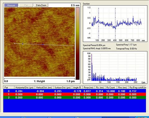
AFM pictures show how the surface roughness is dependent on the process parameters.
For the sputter process, the effect and argon pressure can be set to different values. Depending on the process parameters, the deposited layers will have different characteristics: the roughness, grain size and uniformity may be differnt.
Effect 150 W, pressure 1*10-3 mbar
With use of the settings 150W and 1*10-3 mbar, a surface with low roughness is deposited.

Measurement done September 2008, KNIL.
