Specific Process Knowledge/Characterization/Sample preparation: Difference between revisions
| Line 87: | Line 87: | ||
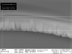
Bird View. Dark area is Silicon. Bright area is Silicon Dioxide. The edges are nicely defined, though corrugated on the 100 nm scale. | Bird View. Dark area is Silicon. Bright area is Silicon Dioxide. The edges are nicely defined, though corrugated on the 100 nm scale. | ||
]] | ]] | ||
![[image: | ![[image:StackedSlicesWithFrame.jpg|300x300px|thumb|left| | ||
Close up. Bird View. Dark area is Silicon. Bright area is Silicon Dioxide. Residues of the SiO2 etching are apperent on top of the SiO2, i.e. particles a few nanometers in diameter. Most probably it is sputtered and redopsited Silicon Dioxide, but not confirmed. Attempts to remove them in 7-Up or HCl failed. | Close up. Bird View. Dark area is Silicon. Bright area is Silicon Dioxide. Residues of the SiO2 etching are apperent on top of the SiO2, i.e. particles a few nanometers in diameter. Most probably it is sputtered and redopsited Silicon Dioxide, but not confirmed. Attempts to remove them in 7-Up or HCl failed. | ||
]] | ]] | ||
![[image: | ![[image:WaferWithCast.jpg|300x300px|thumb|left| | ||
Tilt angle 20 degree. Close up. Bird View. Dark area is Silicon. Bright area is Silicon Dioxide. The Silicon Dioxide sidewall is corrugated. | Tilt angle 20 degree. Close up. Bird View. Dark area is Silicon. Bright area is Silicon Dioxide. The Silicon Dioxide sidewall is corrugated. | ||
]] | ]] | ||
Revision as of 19:30, 12 May 2015
Replica Molding for Sample Inspection
by Frederik Stöhr @danchip
Introduction
Negative replicas of micro- or nanostructures can be obtained by casting with PDMS. This can facilitate the characterization of the three dimensional shape, the texture, or the roughness of a given sample. It may circumvent the inabilities of probes (AFM tip, stylus) to approach a surface of e.g. a deep and narrow cavity. It may also circumvent limitations of the optical profiler regarding the maximum detectable slope or the sensitivity of the CCD when measuring strongly tapered or deep cavities. PDMS is a common material in microfabrication and has unique properties that allow replicating features in the single nanometer range [1].
- A simplified list of necessary steps is given below.
- Please follow the safety and working rules of the individual lab the work is done in and consider the safety instructions given in [2].
- There is a dedicated lab for work with PDMS at DTU Nanotech.
- Please be aware that it is not allowed to work with PDMS in its uncured state inside the cleanroom. The list of approved chemicals inside the cleanroom still holds.
- Details on Danchip’s experience with PDMS as a casting material may be found in [3] (please cite!). A detailed description for PDMS casting can be found in [2] and practical information is given in [4].
- The most important steps for obtaining high quality casts are the thorough mixing of the two components of the PDMS Kit (Sylgard 184, Dow Corning) and the sufficient outgassing of the polymer prior and after pouring the polymer into the mould. The house vacuum may be too weak. For special demands, try to get hold of a separate pump like a HiCube Classic from Pfeiffer Vacuum [4] (there is one around at DTU Photonics or Danchip).
- The application of an anti-stiction coating, like FDTS, is necessary. It may be applied inside the cleanroom by the MVD. Contact the respective person.
- The mold may be reused upon casting without deterioration (try!)
A simplified list of necessary steps
| Step | Task | Aim | Methods |
|---|---|---|---|
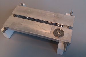
| 1 | Sample preparation | A mold containing the sample that is sufficiently sealed to allow holding the viscous polymer. | Some parts from the mechanical workshop, etc. Do not forget poper cleaning. |
| 2 | Anti-stiction coating | A sample to which PDMS does not adhere upon casting. | E.g. MVD -> FDTS layer (comply to cleanroom and machine rules) |
| 3 | PDMS mixing | A good PDMS mixture. | The kit, a plastic cup, a spatula and patience. |
| 4 | Mixture Outgassing | A mixture without any air bubbles apparent. | A desiccator. (~10min) |
| 5 | Pouring | The mixture is filled into the structures to be casted. | Gently pour the mixture into the mold. |
| 6 | Sample outgassing. | A sample filled with the mixture without air being trapped somewhere. | A desiccator. (~10min) |
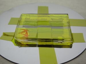
| 7 | Sample curing | A cured PDMS. | An oven (e.g. 5 hours @ 70C) |
| 8 | Sample cooling | A cooled PDMS & sample | ~3 hours @ room temperature |
| 9 | PDMS release | The PDMS cast ready for further usage | Gently detach the cured PDMS from the mold. |
Example: Replica Molding of cross sections of DRIE etched cavities
General Description
- Process date: Feb 2014
- Recipe: m_res_ny@0degrees
- Process time: 5:30 min
- Substrate: 525 µm Si + 1.1 µm thermal silicon oxide + HMDS (adhesion promoter)
- Mask: [XOP3] AZ positive resist 1.5 µm thick (6-inch aligner 3 sec exposure, 60 sec developer)
- Etch Load (Total Exposed SiO2): ~ 10 %
- Post process: O2 Plasma Ashing 10 min
References
[1] Polymer Imprint Lithography with Molecular-Scale Resolution
[2] Soft lithography for micro- and nanoscale patterning
[3] How to do PDMS lithography replication from a SU-8 mold?
[4] Research on the cast molding process for high quality PDMS molds


