Specific Process Knowledge/Lithography/CSAR: Difference between revisions
| Line 553: | Line 553: | ||
! width=15%| | ! width=15%| | ||
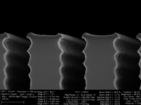
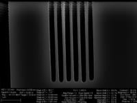
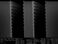
! colspan="4"| SEM inspection of wafer 4.09, 20 nm exposed pattern, shot pitch 5 nm | ! colspan="4"| SEM inspection of wafer 4.09, 20 nm exposed pattern, shot pitch 5 nm | ||
|- | |- | ||
|- | |- | ||
Revision as of 10:29, 12 January 2015
| Resist | Polarity | Manufacturer | Comments | Technical reports | Spinner | Developer | Rinse | Remover | Process flows (in docx-format) |
| CSAR | Positive | AllResist | Standard positive resist, very similar to ZEP520. | Allresist_CSAR62_English.pdf,, CSAR_62_Abstract_Allresist.pdf | Manual Spinner 1 (Laurell), Spin Coater Labspin | XAR-600-546, XAR-600-548, N50, MIBK:IPA | IPA | AR-600-71, 1165 Remover | Process_Flow_CSAR.docx |
Simple e-beam pattern in this resist has been tested, the results showed on this page. If you have questions to the process or wish to use this e-beam resist, please contact Tine Greibe at tigre@danchip.dtu.dk.
Process Flow
| Equipment | Process Parameters | Comments | |
|---|---|---|---|
| Pretreatment | |||
| 4" Si wafers | No Pretreatment | ||
| Spin Coat | |||
| Spin Coater Manual, LabSpin, A-5 | AR-P 6200/2 AllResist E-beam resist
60 sec at various spin speed. Acceleration 4000 s-2, softbake 1 - 5 min at 150 deg Celcius |
Disposal pipette used; clean by N2-gun before use. Use approximately 1.5 ml per 4" wafer, never use a pipette twice. Softbake is not a crucial step, see e-mail correspondence with AllResist here. | |
| Characterization | |||
| Ellipsometer VASE B-1 | 9 points measured on 100 mm wafer | ZEP program used; measured at 70 deg only | |
| E-beam Exposure | |||
| JEOL 9500 E-beam writer, E-1 | Dosepattern 15nm - 100nm,
dose 120-350 muC/cm2 |
Virtual chip mark height detection (CHIPAL V1) used in corner of every dose array | |
| Development | |||
| Fumehood, D-3 | 60 sec in X AR 600-546,
60 sec rinse in IPA, N2 Blow dry |
Gentle agitation while developing. After developing, wafer is immersed in beaker with IPA, subsequently blow dried with N2 gun. | |
| Characterization | |||
| Zeiss SEM Supra 60VP, D-3 | 2-3 kV, shortest working distance possible, chip mounted with Al tape | For dosepattern SEM inspection: the wafers are diced into smaller pieces and sputter coated with Pt at DTU CEN before SEM inspection; please contact Ramona Valentina Mateiu for further information. | |
Spin Curves
The thickness is measured on VASE Ellipsometer using a simple Cauchy model for a transparent polymer on Si. The measurements are performed at one incidence angle (70 degrees) only. 9 points on each 4" wafer has been measured; the standard deviation thus representing the homogeinity of the film on the 4" wafers.
Please be aware that I have experienced a somewhat large thickness deviation (5-8 %) depending on the amount of resist applied to the wafer before spin coating.
Dosepattern has been e-beam exposured and SEM inspected on those wafers marked by silver gray.
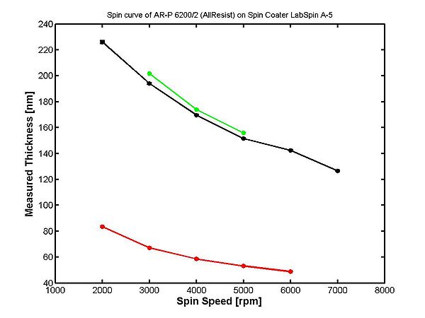
| AllResist AR-P 6200 (> 2ml per 4" wafer) spinning on Spin Coater: Manual LabSpin A-5, TIGRE, 09-04-2014. Softbake 5 min @ 150 degC. | ||||||
|---|---|---|---|---|---|---|
| Spin Speed [rpm] | Acceleration [1/s2] | Thickness [nm] | St Dev | |||
| 2000 | 4000 | 225.98 | 0.97 | |||
| 3000 | 4000 | 194.00 | 0.6 | |||
| 4000 | 4000 | 169.57 | 0.32 | |||
| 5000 | 4000 | 151.47 | 0.26 | |||
| 6000 | 4000 | 142.38 | 0.41 | |||
| 7000 | 4000 | 126.59 | 0.36 | |||
| AllResist CSAR (< 2ml per 4" wafer) on Spin Coater: Manual LabSpin A-5, TIGRE, 16-06-2014. Softbake 2 min @ 150 degC. | ||||||
|---|---|---|---|---|---|---|
| Spin Speed [rpm] | Acceleration [1/s2] | Thickness [nm] | St Dev | |||
| 3000 | 4000 | 201.61 | 1.20 | |||
| 4000 | 4000 | 173.89 | 0.64 | |||
| 5000 | 4000 | 155.91 | 0.65 | |||
| AllResist CSAR 1:1 in anisole (< 2ml per 4" wafer), Spin Coater: Manual LabSpin A-5, TIGRE, 16-06-2014. Softbake 2 min @ 150 degC. | ||||||
|---|---|---|---|---|---|---|
| Spin Speed [rpm] | Acceleration [1/s2] | Thickness [nm] | St Dev | |||
| 2000 | 4000 | 83.48 | 0.49 | |||
| 3000 | 4000 | 67.12 | 0.41 | |||
| 4000 | 4000 | 58.64 | 0.44 | |||
| 5000 | 4000 | 53.13 | 0.39 | |||
| 6000 | 4000 | 48.76 | 0.38 | |||
Contrast Curves
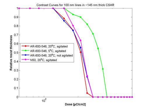
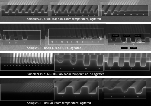
100 nm lines in ~145 nm thick CSAR has been developed with AR-600-546 (standard CSAR developer) with and without agitation at room temperature and at 5 degrees Celsius. Furthermore, same pattern ahs been developed with N50 (standard developer for ZEP520A).
| wafer 9.19 Contrast Curve, Processed by TIGRE, Dec-Jan 2014-2015 | ||||
|---|---|---|---|---|
| Resist | Spin Coat | E-beam exposure | Development | Characterisation |
| CSAR AR-P6200 AllResist | 19-12-2014, LabSpin A-1, 4000 rpm, 60s, softbaked 60s @ 150degC | 19-12-2014, JBX9500 E-2, 2nA aperture 5, doses 60-600 µC/cm2, 100 nm lines and spaces | 22-12-2014, 05-01-2015, Fumehood D-2, misc developers, rinsed in IPA 60s. The cold development was performed with developer stored in refrigerator (Cx1), exact temperature was not measured. | 23-12-2014, 05-01-2015, Zeiss Supra 60VP, 10kV, Inlens detector, stage at - 4-5 degrees. Samples not coated before inspection. |
Dosetests
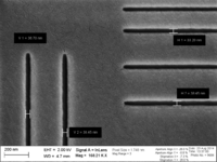
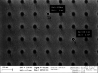
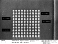
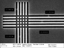
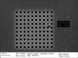
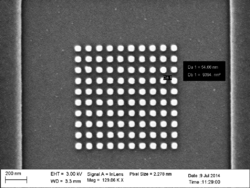
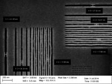
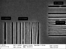
So far (September 2014) three wafers with CSAR have been e-beam exposed with dosetests and inspected in SEM. Thickness of resist, e-beam dose and development time has been changed somewhat from wafer to wafer:
style = "border-radius: 6px; border: 3px solid #000000;
| Process | Equipment | Parameters | ||
|---|---|---|---|---|
| 6.13 | 4.09 | 3.05 | ||
| Resist | Fumehood D-3 | Resist: AR-P 6200/2 diluted 1:1 in anisole (Bottled opened 16-06-2014 TIGRE) | Resist: AR-P 6200/2 diluted 1:1 in anisole (Bottled opened 16-06-2014 TIGRE) | Resist: AR-P 6200/2 |
| Spin Coat | Spin Coater LabSpin A-5 | Spin: 1 min @ 6000 rpm, softbake: 1 min @ 150 degC, thickness: ~50nm (27-08-2014 TIGRE) |
Spin: 1 min @ 5000 rpm, softbake: 2 min @ 150 degC, thickness: ~53nm (16-06-2014 TIGRE) |
Spin: 1 min @ 6000 rpm, softbake: 5 min @ 150 degC, thickness: ~143nm (09-04-2014 TIGRE) |
| E-beam exposure | JEOL 9500 E-2 | Condition file: 0.2nA_ap5, doses: 180-420 muC/cm2, Shot pitch: 7-27 nm, PEC: no (27-08-2014 TIGRE) |
Condition file: 0.2nA_ap5, doses: 207-242 muC/cm2, Shot pitch: 5 nm, PEC: no (02-07-2014 TIGRE) |
Condition file: 2nA_ap5, doses: 207-242 muC/cm2, Shot pitch: 5 nm, PEC: no (10-04-2014 TIGRE) |
| Develop | Fumehood D-3 | Developer: SX-AR 600-54/6, time: 30 sec, Rinse: 30 sec in IPA (28-08-2014 TIGRE) |
Developer: SX-AR 600-54/6, time: 60 sec, Rinse: 30 sec in IPA (08-07-2014 TIGRE) |
Developer: SX-AR 600-54/6, time: 60 sec, Rinse: 60 sec in IPA (April/May-2014 TIGRE) |
| Sputter Coat (please contact Ramona Valentina Mateiu for information ) | Cressington 208HR, DTU CEN | 3-5 nm Pt, sputtering, (29-08-2014 TIGRE) | 3-5 nm Pt, sputtering (09-07-2014 TIGRE) | 3-5 nm Pt, sputtering (22-05-2014 TIGRE) |
| Characterization | Zeiss SEM Supra 60VP, D-3 | Acc voltage: 3 kV, WD: < 4mm, conducting tape close to pattern (29-08-2014 TIGRE) |
Acc voltage: 3 kV, WD: < 4mm, conducting tape close to pattern (09-07-2014 TIGRE) |
Acc voltage: 2 kV, WD: < 4mm, conducting tape close to pattern (06-06-2014 TIGRE) |
SEM inspection
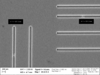
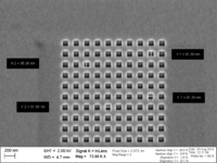
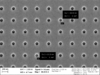
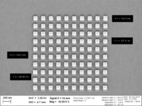
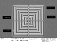
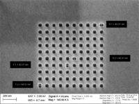
| SEM inspection of wafer 6.13, 100 nm exposed pattern, shot pitch 7 nm | |||||||
|---|---|---|---|---|---|---|---|
| 300 [muC/cm2] | 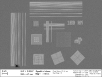
|
|
|
|
|
|
ACHK NOT READY |
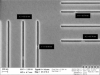
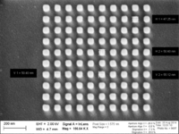
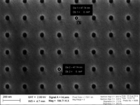
| SEM inspection of wafer 6.13, 50 nm exposed pattern, shot pitch 7 nm | |||||||
|---|---|---|---|---|---|---|---|
| 270 [muC/cm2] | 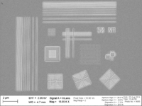
|
|
|
|
|
ACHK NOT READY | |
| 300 [muC/cm2] | 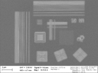
|
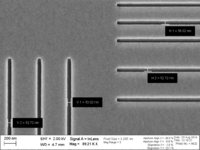
|
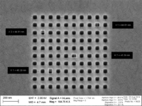
|
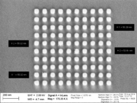
|
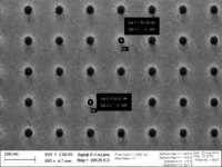
|
ACHK NOT READY | |
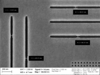
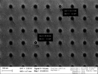
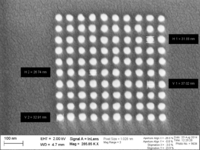
| SEM inspection of wafer 6.13, 30 nm exposed pattern, shot pitch 7 nm | |||||||
|---|---|---|---|---|---|---|---|
| 270 [muC/cm2] | 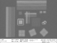
|
|
|
|
ACHK NOT READY | ||
| 300 [muC/cm2] | 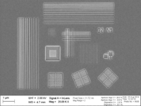
|
|
|
|
ACHK NOT READY | ||
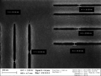
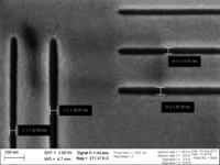
| SEM inspection of wafer 6.13, 20 nm exposed pattern, shot pitch 7 nm | ||||
|---|---|---|---|---|
| 270 [muC/cm2] | 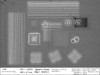
|
|
ACHK NOT READY | |
| 300 [muC/cm2] | 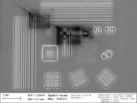
|
|
ACHK NOT READY | |
| SEM inspection of wafer 4.09, 50 nm exposed pattern, shot pitch 5 nm | ||||||
|---|---|---|---|---|---|---|
| 230 [muC/cm2] | 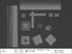
|
|
|
|
| |
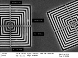
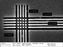
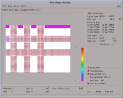
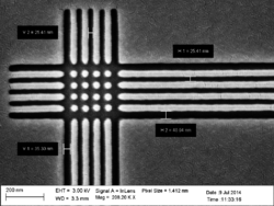
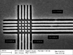
| SEM inspection of wafer 4.09, 30 nm exposed pattern, shot pitch 5 nm | ||||
|---|---|---|---|---|
| 219 [muC/cm2] | 
|
|
| |
| 230 [muC/cm2] | 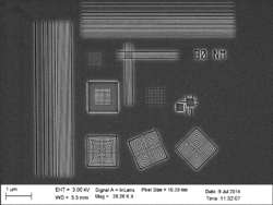
|
|
||
| 242 [muC/cm2] | 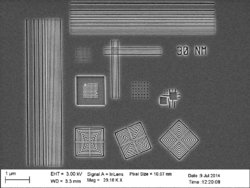
|
|
||
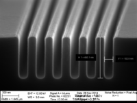
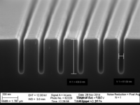
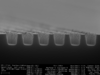
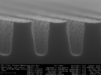
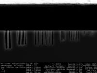
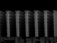
| SEM inspection of wafer 4.09, 20 nm exposed pattern, shot pitch 5 nm | ||||
|---|---|---|---|---|
| 242 [muC/cm2] | 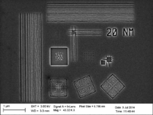
|
|
||
| 253 [muC/cm2] | 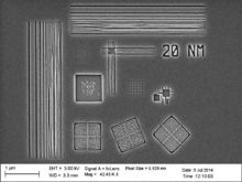
|
|
||
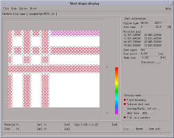
| SEM inspection of wafer 4.09, 15 nm exposed pattern, shot pitch 5 nm | ||||
|---|---|---|---|---|
| 253 [muC/cm2] | 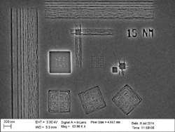
|
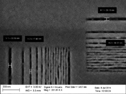
|
| |
| 276 [muC/cm2] | 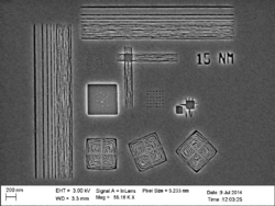
|
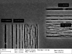
|
||
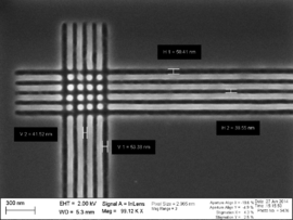
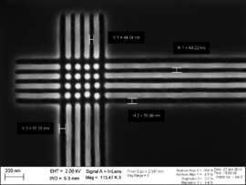
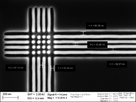
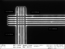
| SEM inspection of wafer 3.05, 50 nm exposed pattern, shot pitch 5 nm | ||||
|---|---|---|---|---|
| 207 [muC/cm2] | 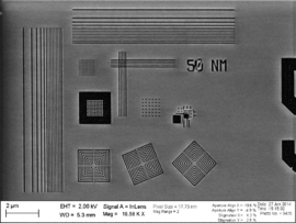
|
|
NO ACHK READY | |
| 219 [muC/cm2] | 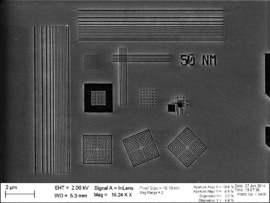
|
|
||
| 230 [muC/cm2] | 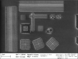
|
|
||
| 242 [muC/cm2] | 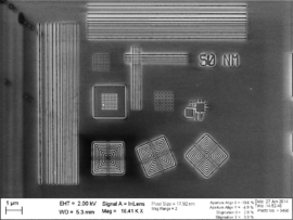
|
|
||
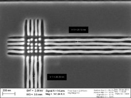
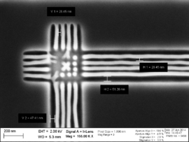
| SEM inspection of wafer 3.05, 30 nm exposed pattern, shot pitch 5 nm | ||||
|---|---|---|---|---|
| 207 [muC/cm2] | 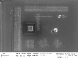
|
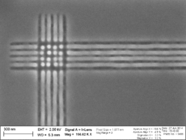
|
NO ACHK READY | |
| 219 [muC/cm2] | 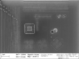
|
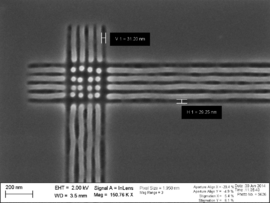
|
||
| 230 [muC/cm2] | 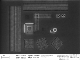
|
|
||
| 242 [muC/cm2] | 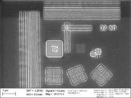
|
|
||
| SEM inspection of wafer 3.05, 20 nm exposed pattern, shot pitch 5 nm | ||||
|---|---|---|---|---|
| 207 [muC/cm2] | 
|

|
NO ACHK READY | |
| 230 [muC/cm2] | 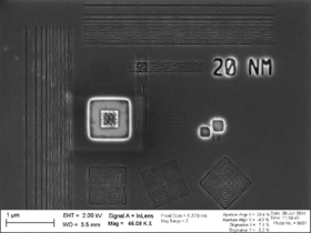
|
|||
| 242 [muC/cm2] | 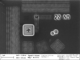
|
|||
| 253 [muC/cm2] | 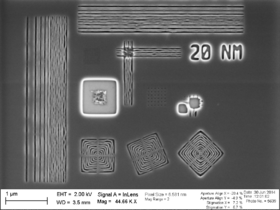
|
|||
Etch Tests
If you have wafers or chips with CSAR you would like to have tested, please send me an [email].
Chlorine versus flourine-based etches
We have experienced problems with removal of CSAR after chlorine-based dry etch, see the file File:DryEtchTestsCSAR.pdf. It seems the chlorine etch forms particles of chlorinated CSAR on the surface, and these particles remains on the surface after resist removal with AR-600-71. The C4F8/SF6 etch also forms particles on the surface, but much smaller than those formed in the chlorine etch. It seems these particles are removed after 3 minutes in AR-600-71.
How to mount chips in dry etch tools
All etch rates presented here are measured on chips (i.e. diced 4" wafers) crystal bonded to a carrier. The carrier is either a blank Si wafer, a Si wafer spin coated with resist or a Si wafer coated with ALD grown Al2O3.
| Sample | CSAR Etch rate nm/min |
|---|---|
| Full 4" Si wafer with non-patterned ~180 nm CSAR | ~56.5 (based on 2 runs) |
| Full 4" Si wafer with non-patterned ~240 nm CSAR, postbaked 60 sec @ 130 degC |
~56.5 (based on 2 runs) |
| 1/4 4" Si wafer with non-patterned ~125 nm CSAR, not crystal bonded to Si carrier |
~83.3 (based on 3 runs) |
| 1/4 4" Si wafer with non-patterned ~125 CSAR, crystal bonded to 4" Si carrier |
~54 (based on 1 run) |
Etch rates and profile inspection
Continous Etches

