Specific Process Knowledge/Etch/Wet Polysilicon Etch: Difference between revisions
| Line 16: | Line 16: | ||
===PolySi Etch data=== | ===PolySi Etch data=== | ||
{| border=" | {| border="2" cellspacing="0" cellpadding="4" align="left" | ||
! | ! | ||
! PolySi Etch @ room temperature | ! PolySi Etch @ room temperature | ||
|- | |- | ||
|General description | |'''General description''' | ||
| | | | ||
Etch of poly-si/Si(100) | Etch of poly-si/Si(100) | ||
|- | |- | ||
|Chemical solution | |'''Chemical solution''' | ||
|HNO<sub>3</sub> : BHF : H<sub>2</sub>O (20 : 1 : 20) | |HNO<sub>3</sub> : BHF : H<sub>2</sub>O (20 : 1 : 20) | ||
|- | |- | ||
|Process temperature | |'''Process temperature''' | ||
|Room temperature | |Room temperature | ||
|- | |- | ||
|Possible masking materials | |'''Possible masking materials''' | ||
| | | | ||
*Photoresist(min. 2.2 µm is recommended) | *Photoresist(min. 2.2 µm is recommended) | ||
*LPCVD-oxide (TEOS) | *LPCVD-oxide (TEOS) | ||
|- | |- | ||
|Etch rate | |'''Etch rate''' | ||
| | | | ||
*R<sub>Si</sub> ~1000-2000 Å/min (depending on doping level) | *R<sub>Si</sub> ~1000-2000 Å/min (depending on doping level) | ||
| Line 42: | Line 42: | ||
*Photoresist (2.2 µm) withstand ~20-30 min | *Photoresist (2.2 µm) withstand ~20-30 min | ||
|- | |- | ||
|Batch size | |'''Batch size''' | ||
| | | | ||
1-25 wafers at a time | 1-25 wafers at a time | ||
|- | |- | ||
|Size of substrate | |'''Size of substrate''' | ||
| | | | ||
2-4" wafers | 2-4" wafers | ||
|- | |- | ||
|} | |} | ||
Revision as of 14:05, 31 January 2008
Wet PolySi Etch

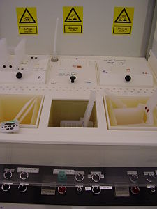
The wet PolySi Etch is an isotropic silicon etch. This holds for both a poly-silicon thin-film as well as single-crystalline material such as a Si(100) surface. The PolySi Etch process is placed in a dedicated PP-tank in a laminar-flow bench in cleanroom 4.
The PolySi Etch is typically used for opening holes in poly-silicon thin-films, using photoresist as an etch mask. Due to its isotropic nature the under-etching (etch-bias) at least amounts to the thickness of the poly-silicon layer. Another example of usage is etching of "circular-shaped" holes in silicon substrates.
The PolySi Etch is based on the combined oxidation of silicon followed by dissolution of the silicon oxide. The etch solution consists of:
HNO3 : BHF : H2O - (20 : 1 : 20)
NB: The life time of the solution is only a few days.
PolySi Etch data
| PolySi Etch @ room temperature | |
|---|---|
| General description |
Etch of poly-si/Si(100) |
| Chemical solution | HNO3 : BHF : H2O (20 : 1 : 20) |
| Process temperature | Room temperature |
| Possible masking materials |
|
| Etch rate |
|
| Batch size |
1-25 wafers at a time |
| Size of substrate |
2-4" wafers |
