Specific Process Knowledge/Lithography/Baking: Difference between revisions
| Line 91: | Line 91: | ||
Film or pattern of all types | Film or pattern of all types | ||
| | | | ||
Silicon, glass, and polymer substrates | |||
Film or pattern of all types except type IV | |||
| | | | ||
All substrates | |||
Film or pattern of all types | |||
| | |||
Silicon, glass, and polymer substrates | |||
Film or pattern of all types | |||
| | |||
Silicon, glass, and polymer substrates | |||
Film or pattern of all types | |||
| | |||
Silicon, glass, and high Tg polymer substrates | |||
Film or pattern of all types except resist | |||
|- | |- | ||
|-style="background:WhiteSmoke; color:black" | |-style="background:WhiteSmoke; color:black" | ||
!Restrictions | !Restrictions | ||
| | | | ||
| | |III-V, copper, steel substrates and Pb, Te films | ||
|Information is given at the individual hotplate | |||
|III-V substrates and Pb, Te films | |||
|III-V, copper, steel substrates | |||
|Resist is not allowed | |Resist is not allowed | ||
|- | |- | ||
Revision as of 12:48, 4 November 2014
Feedback to this page: click here
Comparing baking methods
| Hotplate: 90-110C | SU8 hotplates | Fumehood hotplates | Oven 90C | Oven: 120C - 250C | Oven 250C | |
|---|---|---|---|---|---|---|
| Use |
Soft bake Post-exposure bake (PEB) |
Soft bake Post-exposure bake (PEB) |
Soft bake |
Soft bake |
Hard bake |
Dehydration |
| Temperature |
Maximum 120°C |
Maximum 250°C |
Maximum 250°C |
Fixed 90°C |
120 - 250°C |
Fixed 250°C |
| Substrate size |
|
|
|
|
|
|
| Allowed materials |
Silicon, glass, and polymer substrates Film or pattern of all types |
Silicon, glass, and polymer substrates Film or pattern of all types except type IV |
All substrates Film or pattern of all types |
Silicon, glass, and polymer substrates Film or pattern of all types |
Silicon, glass, and polymer substrates Film or pattern of all types |
Silicon, glass, and high Tg polymer substrates Film or pattern of all types except resist |
| Restrictions | III-V, copper, steel substrates and Pb, Te films | Information is given at the individual hotplate | III-V substrates and Pb, Te films | III-V, copper, steel substrates | Resist is not allowed |
Hotplates
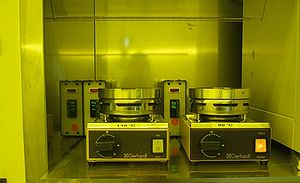
Hotplate: 90-110C

Hotplate: 90-110C is used for baking of 2" - 6" wafers.
The user manual, and contact information can be found in LabManager: Hotplate: 90-110C
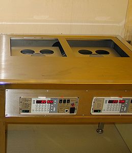
SU8 hotplates

We have two dedicated SU-8 hotplates in C-1.
Users can control the ramp-time, the baking temperature, and the baking time.
The user manual, and contact information can be found in LabManager: Hotplate 1 (SU8) Hotplate 2 (SU8)
Fumehood hotplates

Variable temperature hotplate mostly used for baking of single wafers as a soft baking step after a spin coating of photoresist.
Ovens
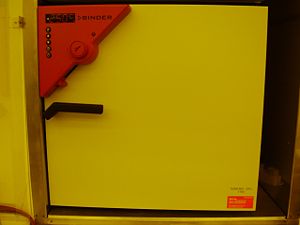
Oven 90C

The oven is mostly used for baking of several wafers at a time at 90 °C as a soft baking step after a spin coating of photoresist. For 1.5µm resist the baking time is 30 min. For most of the other resist thicknesses it is also 30 min.
The user manual, and contact information can be found in LabManager: Oven 90C
Oven: 120C - 250C
The user manual, and contact information can be found in LabManager: Oven: 120C - 250C
Oven 250C for pretreatment

See Oven 250C
